How we can help:
We’ve developed a deep understanding of how the NI FlexRIO interfaces to high-end sub-systems to enable automated test & analysis, capitalizing on our knowledge bank of coding nuances and high-speed interface design.
Want more proof points? Check out these FlexRIO case studies:
Automated production test of EO/IR imaging subsystem
Automated production test of EO/IR imaging subsystem
Assessing quality of mission-critical electronics for imaging
Increased throughput by automated signal skew adjustment and pixel verification
Client – Worldwide supplier of products for aerospace and defense
Challenge
Our client wanted a test system that would significantly increase production rates for a very specialized focal plane array (FPA) and associated readout integrated circuit (ROIC) electronics.
In broad strokes, the system needed to support the following:
- Increase production test throughput as much as reasonably possible within budget and schedule constraints.
- Provide some low-code or no-code way to create new test protocols.
- Protect the DUT using hardware and software interlocks.
- Verify the correctness of test image(s) and all its pixels.
Solution
The FPA and ROIC testing for this client used many of the same techniques we have implemented for FPA/ROIC testers at some of our other clients. Thus, the solution was built around our AEDIS platform and some custom connectivity hardware which paired the DUT to the AEDIS hardware.
Specifically, the test needed to:
- Send digital signals from the AEDIS hardware to initiate and coordinate the test steps.
- De-skew bitstreams from the DUT.
- Organize and rearrange the bitstreams into image pixels.
- Provide custom “personality” modules to connect the DUT and AEDIS hardware.
- Protect the DUT from connection and power faults.
Benefits
All the bulleted items above are common requests from our clients and are supplied with the AEDIS platform or easily accommodated by design of the platform. Consequently, AEDIS often meets 80% or even 90% of typical client needs.
Thus, the client was able to cost-justify an AEDIS-based solution for two main reasons:
- overall system costs for an AEDIS-based solution were significantly less than a completely custom system and
- the increased production rates provided plenty of schedule buyback.
Furthermore, the script-based, low-code capabilities offered by AEDIS enabled:
- Support of different test images.
- Control of image transfer initiation, handling responses from the DUT, and flow.
- Version control (by the client) of script-based test configurations.
- Defined parsing of bitstreams to create the image pixels to simplify downstream image collection.
System Overview
The test system was built around AEDIS, which is a combination of five major components:
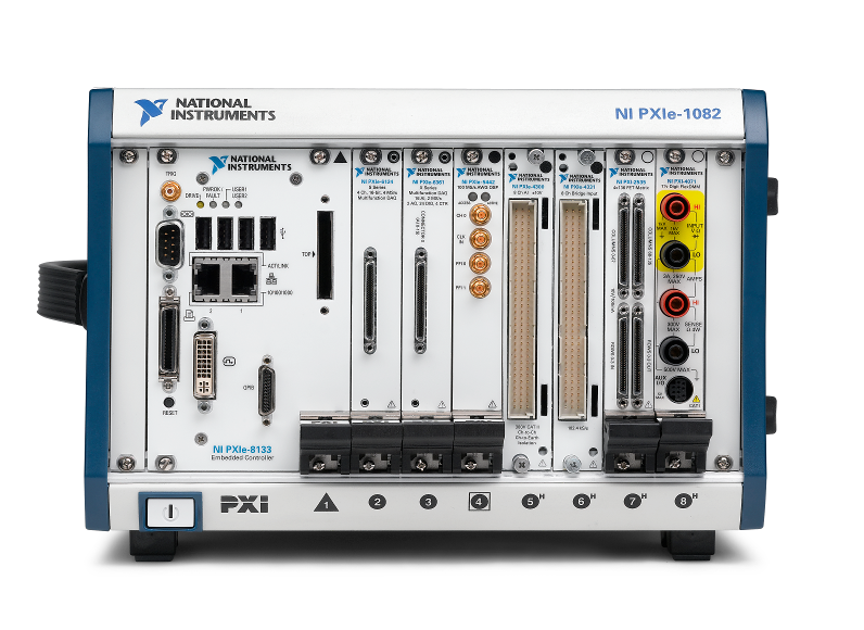
- NI FlexRIO PXI modules and chassis.
- Signal conditioning hardware.
- A REST API interface for the client’s test sequencer and LabVIEW FPGA for the hardware interfacing.
- An out-of-the-box browser-based app to interact with the AEDIS system.
- A source measure unit to supply and test the DUT’s power needs.
With this design, AEDIS acts as an instrument to incorporate into the client’s overall test system.
The NI FlexRIO modules use Xilinx FPGAs for digital I/O at the rates and channel counts required to fully test the FPA on the DUT. Some digital lines were used for commands to the FPA while most were used to receive output from the FPA.
The AEDIS interfacing hardware acts as an ITA while converting the FPA/ROIC signals to types expected by the FlexRIO. A custom “personality” module provides the physical connectivity from the client’s hardware cabling to the ITA. The AEDIS software handles the test configuration setup, data acquisition, and data storage via high-speed RAID drives.
During development of the test system, AEDIS hardware and software were also used to emulate the actual FPA and electronics to verify, before deployment, that the test system was working as required. This same setup can also be used for periodic verification as might be needed for an annual equipment performance audit.
Finally, configuration files were built from user-created scripts to give the client flexibility for adding new test capabilities for the DUT.
Some of the significant hardware and software challenges mitigated by this combination of PXI FlexRIO and AEDIS are:
- Interface to tester: The AEDIS system is treated as an instrument managed by an overall test system. The client developed some custom C# code to interface to the AEDIS REST API interface to automate their test procedures.
- DUT interfacing: Standard (keyed) cabling ran between the DUT and the custom AEDIS “personality” card to match cabling to the DUT. The output of this personality module went to the AEDIS LVDS modules.
- Channel skew: The high-frequency digital LVDS signals from the DUT can develop noticeable timing skews between channels upon arrival at the FlexRIO inputs due to signal path length differences. The test system had to detect and accommodate for these skews before combining the bits streams into bytes, then pixels, then an image.
- High data rates: Not only were the digital data output at high frequency but many channels were needed to accommodate the full frame rate of the DUT. The FPGA and the PXI backplane needed enough processing and transport bandwidth to accommodate the throughput.
- Interlocks: Keyed cabling and “signal present” software checks assured proper connections between the DUT and the AEDIS hardware before testing would begin. These safety checks were justified due to the high cost of each DUT.
- User-defined scripts: Scripts created and edited by the user provided flexibility to address future test types and system obsolescence. For example, the scripts defined details such as a) the DUT-specific commands (some of which could not be shared with us for secrecy reasons), b) when the image is being captured (or ignored), and c) if the image is stored to disk or RAM.
| SOFTWARE FUNCTIONS |
|---|
| Browser-based app for manual operation and recipe creation and editing |
| REST API interface for support of automated operation |
| Configuration of the test via scripts |
| Pre-test interlock checks |
| Data collection, bit stream processing, and mapping digital bitstream to pixels |
| HARDWARE USED |
|---|
| Standard AEDIS components for signal buffering, conditioning, and signal acquisition |
| Custom personality hardware for connectivity and physical connection interlocks |
| Signal test points in AEDIS breakout ITA modules enabled use of a logic analyzer for troubleshooting and further verification |
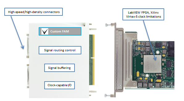
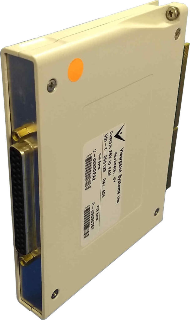
Custom FlexRIO Adaptor Module supports HIL Test Upgrade
Custom FlexRIO Adaptor Module supports HIL Test Upgrade
A custom-COTS approach reduces cost and delivery time.
Client – Major National Research Lab

Challenge
Our client has a client (the end-user) for which they developed an HIL test system several years prior. Parts were obsolete and the system needed an upgrade. The prior system had many custom-designed electronic components which could not be replaced without a complete redesign.
Consequently, our client wanted to use COTS. However, one device needed 28 VDC digital I/O, a couple of lines which carried significant current (amp, not milliamp, levels) and at switching rates much higher than a COTS solid state relay could provide.
Solution
Viewpoint reviewed the requirements and created a hybrid COTS-custom solution. We combined an NI FlexRIO module with a custom FlexRIO Adapter Module (FAM) for the front end to satisfy the 28 VDC signals levels and required current drive.
Benefits
- COTS FlexRIO integrates into the remainder of our client’s PXI-based test system.
- The Custom I/O was designed for flexibility. Our client can use this FAM for both their initial end-user and other programs / clients too.
- Reduced cost relative to a completely custom solution.
- Delivery time reduced by months relative to a custom solution
FAM Overview
The custom FAM interfaced with the NI FlexRIO module, which offered low-level digital I/O (3.3 V logic), to digital signal conditioning hardware that provided the 28 VDC signal levels and required current drive.
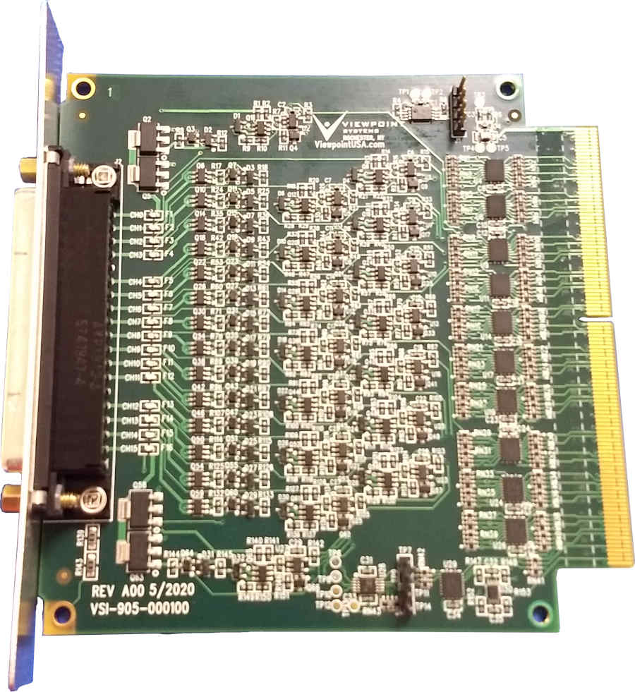
Each I/O pin was configurable as input or output (source or sink). Each bank of 4 channels had an adjustable threshold level set via an adjustable DAC output. Some of the channels are designed for amp-level current drive, while the remainder were 250 mA. All I/O was fused appropriately.
Viewpoint also developed LabVIEW FPGA and VHDL to enable our client and the end-user to:
- Configure the I/O as in or out.
- Communicate to the DAC to allow custom input threshold trigger levels.
- Read and write the digital data.
| SOFTWARE FUNCTIONS |
|---|
| Set the direction of each of the DIO channels |
| Set the threshold level on the input channels |
| Read / Write DIO Data |
| End User Application |
| HARDWARE UTILIZED |
|---|
| COTS NI FlexRIO |
| Custom FlexRIO Adaptor Module(FAM) |
| INTERFACES / PROTOCOLS |
|---|
| Customized VHDL Component Level Intellectual Property (CLIP) integrated with LabVIEW FPGA |
| LabVIEW FPGA as required along with LabVIEW and TestStand |
High-Speed Digital Subsystem Emulator
High-Speed Digital Subsystem Emulator
Client: A large company involved in C4ISR
At maximum throughput, the AEDIS systems needed to consume and produce more than about 800 MB/s/slot.
Background
A large company involved in C4ISR was developing a system for a new high-speed digital sensor device. Viewpoint was contracted to build a test system used in design validation and ultimately endurance testing of the sensor. Since the sensor was a component of a larger system which was being developed at the same time, another test system was created to simulate the sensor by feeding signals into the system. This ability to use HIL testing for both the sensor and the downstream sensor electronics enabled parallel development, thus saving time and reducing schedule.
Challenge
Both the amount of data and the frequencies of the various digital signals were nearly at the limit of hardware capabilities. At maximum throughput, the systems needed to consume during record and produce during playback about 800 MB/s/slot. The FPGA clock on the FlexRIO had to run up to 300 MHz. The skew between triggers for data transmission needed to be less than 5 ns even between multiple FlexRIO cards even when the parallel data paths have inherent skews associated with the sensor. Finally, the systems needed to handle clocks that might be out-of-phase.
Achieving these requirements required significant engineering design in the face of multiple possible roadblocks, any one of which could have eliminated a successful outcome.
Furthermore, as usual, the development timeline was tight. In this case, it was a very tight 3 months. Basing the solution on our AEDIS platform was critical to meeting this challenge.
Viewpoint’s Solution
To meet the timeline, we had to work in parallel across several fronts:
- LabVIEW-based application development for both record and playback
- LabVIEW FPGA development for marshalling data between the controller and DRAM
- Custom FAM circuit board design and build
- FlexRIO FPGA CLIP nodes and code for low-level data handling
Technical Highlights
This sensor had several parallel data paths of clock and data lines with clock speeds up to 300 MHz on each path requiring exacting design and build of a custom FlexRIO Adapter Module (FAM) and unique custom CLIP nodes for extending the FlexRIO FPGA capabilities. The FAM also had a special connector for interfacing to the customer’s hardware.
Additional NI hardware and software completed the system components.
Results
The choice to base the AEDIS emulators on NI hardware and software was critical to completing this project. The open architecture in both hardware (custom FAM) and software (CLIP Nodes) enabled us to include some very creative extensions to the base toolset without which the project would not have succeeded in the allotted pressured schedule and on a predetermined budget. We were able to stretch the capabilities of the hardware and software very close to their maximum specifications by combining COTS and custom much more cost effectively than a purely custom design. Further, with HIL tests, both the sensor and the sensor electronics could be developed in parallel, leading to a significant schedule buyback for our client.
LabVIEW Layers
The host application, written in LabVIEW, managed the configuration of the data acquisition and the control of the LabVIEW RT-based FlexRIO systems. The configuration primarily dealt with the number of sensor channels in use, skew settings between digital lines, and other parameters that dealt with the organization of the data passed between the sensor and the FlexRIO.
Two FlexRIO applications were written, one for record and one for playback. Each FlexRIO application was written in LabVIEW, and managed the configuration of the FlexRIO cards and the movement of data between the FlexRIO cards and the RAID drives. Note that Windows supported for the RAID driver. Between 10 and 32 DMA channels were used for streaming, depending on the number of sensor channels being used.
And, each FlexRIO application had an FPGA layer, written in LabVIEW FPGA enhanced with custom CLIP nodes. For the record application, we developed a custom DRAM FIFO on the FPGA to assist with the latencies on the PXIe bus. For the playback application, we were able to stream directly from DRAM.
FlexRIO Considerations
The FlexRIO and stock FAMs from NI were initially considered as candidates for this project. Clearly, working with commercial-off-the-shelf (COTS) components would be most effective. Three options were available at the project start which could accommodate the required clock frequencies, but none offered both the required channel counts and skew/routing limitations. Hence, we had to design a custom FAM. This decision, made before the start of the project, turned out to be wise in hindsight because the parallel development path resulted in some shifts of sensor requirements which could be accommodated with the custom FAM but might have led to a dead-end with a COTS FAM.
FlexRIO CLIP
In LabVIEW FPGA, a CLIP Node is a method to import custom FPGA IP (i.e., code) into a LabVIEW FPGA application. CLIP stands for Component-Level Intellectual Property. We needed to use special Socketed CLIP Nodes (i.e., VHDL that can access FPGA pins) for this project because we could expose additional features of the Xilinx Virtex-5 not exposed in LabVIEW FPGA by accessing Xilinx primitives. Some specific features were:
- Faster FPGA clocking
- Additional clocking options
- Individual clock and skew control
- Custom PLL de-jitter nodes
Essentially, the FPGA design had a majority of FPGA code developed in LabVIEW FPGA and we used CLIP Nodes for interfacing the signals between the FlexRIO and the FAM.
FlexRIO Adapter Module
As mentioned earlier, we had to create a custom FAM because of the need to route high speed signals from customer-specific high density connectors while synchronizing signals across multiple data channels and FPGA modules to within one (300 MHz) clock cycle.
At these high-speeds, the FAM needed careful buffering and impedance matching both on the signals as well internal components on the FAM PCB. At the start of the design, we utilized Mentor Graphics HyperLynx High Speed DDR signaling Simulation software to minimize signal reflections prior to building actual hardware. This step saved countless hours in spinning physical hardware designs.
We designed the FAM to allow channel routing and access to additional clock and trigger pins on the Xilinx chip and PXIe backplane.
NI FlexRIO-based Custom Test Equipment for High Speed Digitizer sensor

NI FlexRIO-based Custom Test Stand for High-Speed Digitizer sensor
The initial interface/test system to the DUT was up and running and getting real data from the DUT in ~2 weeks, allowing the customer to maintain a tight development schedule.
Client – A Large Manufacturer
Challenge
Our client was developing an image sensor component and needed to validate the part for a new product line. They wanted to use as much COTs hardware as possible to start testing as soon as possible.
Solution
The custom product validation test equipment utilizes the NI PXI with FlexRIO off-the-shelf hardware combined with custom LabVIEW-based software.
Benefits
- The initial interface/test system to the DUT was up and running and getting real data from the DUT in ~2 weeks, allowing the customer to maintain a tight development schedule.
- Packet Decode completed at FPGA Level allowed error handling and only pertinent data being saved as needed.
- Data Manipulation done at FPGA level for unbundling data into correct disk readable format in real-time.
- All Data captured with TDMS Files to disk enables a higher level of analysis of the data offline.
System Overview
The new PXI-based automated test stand utilizes NI’s FlexRIO with NI stock LVDS FAM.
- Custom VHDL was created to handle the required adjustable delay lines in the data I/O lines and interface to the I/O on the FAM Connector.
- The VHDL interfaced to LabVIEW FPGA which was utilized to stream the data to disk.
- Data is stored onto disk during a test and only the payload data from decoding the protocol is saved.
- The data coming from the UUT is de-packetized and ordered for manipulation downstream.
| SOFTWARE FUNCTIONS |
|---|
| Custom FAM VHDL and LabVIEW FPGA interface Development |
| Custom LVDS Adjustable Delay lines per LVDS Data stream |
| LVDS Buffering |
| Generate multiplied Clock from external clock input to latch in data |
| Source the multiplied clock to Internal LabVIEW FPGA Clock |
| FIFOs for clock domain crossing and DMA |
| High-speed data streaming to Disk |
| LabVIEW RT for example interface to FPGA |
| GUI |
| HARDWARE USED |
|---|
| 19″ rack test stand |
| NI FlexRIO |
| NI FlexRIO FAM – LVDS |
| NI LVDS to flying lead cable |
| NI PXI chassis and controller |
NI FlexRIO enables Device Evaluation & Characterization for high-data-rate sub-system
NI FlexRIO enables Device Evaluation & Characterization for high-data-rate sub-system
100s of man-hours saved in capturing the data.
Client – Automotive Manufacturer
Challenge
New product development drove the need for validation of a new sub-system (a RADAR sensor ) for use in a next-gen system in an automobile. They needed a way to evaluate and characterize the performance of the component under various conditions that were not defined in the UUTs specs. They wanted to use as much COTS hardware as possible for this first run testing because of the expense of a custom test solution and the timeline.
Solution
The NI FlexRIO-based product validation system utilizes COTS hardware, along with some Viewpoint-developed custom software to allow for evaluation and characterization of the UUT.
Benefits
- The utilization of COTs (vs a custom-built FPGA board) test hardware.
- 100s of man-hours saved in capturing the data.
- Allowed customer to manipulate captured data within the LabVIEW environment for more efficient testing, making changes on the fly.
- Error Checking done at the FPGA Level allows for guaranteed valid transfers
- Packet Decode completed at FPGA Level allows for real-time de-packetization for use in storing only payload data.
- All Data captured with TDMS Files for use in over layering different scenarios.
- Scalable to add additional serial data channels allowing for more than one sensor to be captured with a single FlexRIO card.
System Overview
NI’s FlexRIO with NI’s LVDS FAM was used. The NI flying lead cable was utilized initially to connect to the UUT. On the software side custom VHDL was created to handle the 8b/10b serial stream data and clock recovery. The VHDL interfaced to LabVIEW FPGA which was utilized to stream the data to disk on the PXI-based system.
| SOFTWARE FUNCTIONS |
|---|
| Custom FAM VHDL and LabVIEW FPGA interface Development |
| Aurora 8b/10b de-serialization and clock recovery |
| LVDS Buffering |
| Clock to Internal LabVIEW FPGA Clock |
| FIFOs for clock domain crossing and DMA |
| High Speed data streaming to Disk |
| LabVIEW RT for example Interface to FPGA |
| GUI |
| HARDWARE USED |
|---|
| NI FlexRIO |
| NI FlexRIO FAM – LVDS |
| NI LVDS to Flying lead cable |
| NI PXI Chassis and Controller |
| INTERFACES / PROTOCOLS |
|---|
| Aurora 8b/10b |
| TCP/IP |