High-Speed Digital Subsystem Emulator
Client: A large company involved in C4ISR
At maximum throughput, the AEDIS systems needed to consume and produce more than about 800 MB/s/slot.
Background
A large company involved in C4ISR was developing a system for a new high-speed digital sensor device. Viewpoint was contracted to build a test system used in design validation and ultimately endurance testing of the sensor. Since the sensor was a component of a larger system which was being developed at the same time, another test system was created to simulate the sensor by feeding signals into the system. This ability to use HIL testing for both the sensor and the downstream sensor electronics enabled parallel development, thus saving time and reducing schedule.
Challenge
Both the amount of data and the frequencies of the various digital signals were nearly at the limit of hardware capabilities. At maximum throughput, the systems needed to consume during record and produce during playback about 800 MB/s/slot. The FPGA clock on the FlexRIO had to run up to 300 MHz. The skew between triggers for data transmission needed to be less than 5 ns even between multiple FlexRIO cards even when the parallel data paths have inherent skews associated with the sensor. Finally, the systems needed to handle clocks that might be out-of-phase.
Achieving these requirements required significant engineering design in the face of multiple possible roadblocks, any one of which could have eliminated a successful outcome.
Furthermore, as usual, the development timeline was tight. In this case, it was a very tight 3 months. Basing the solution on our AEDIS platform was critical to meeting this challenge.
Viewpoint’s Solution
To meet the timeline, we had to work in parallel across several fronts:
- LabVIEW-based application development for both record and playback
- LabVIEW FPGA development for marshalling data between the controller and DRAM
- Custom FAM circuit board design and build
- FlexRIO FPGA CLIP nodes and code for low-level data handling
Technical Highlights
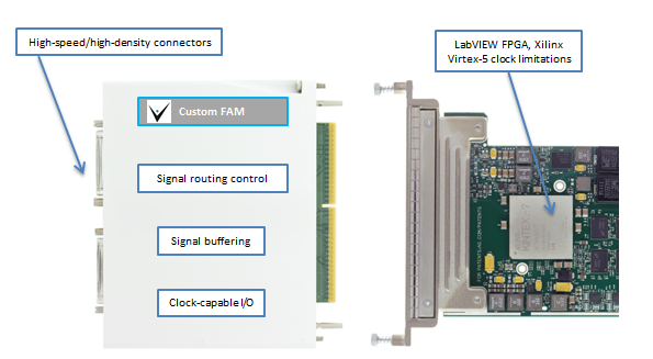
This sensor had several parallel data paths of clock and data lines with clock speeds up to 300 MHz on each path requiring exacting design and build of a custom FlexRIO Adapter Module (FAM) and unique custom CLIP nodes for extending the FlexRIO FPGA capabilities. The FAM also had a special connector for interfacing to the customer’s hardware.
Additional NI hardware and software completed the system components.
Results
The choice to base the AEDIS emulators on NI hardware and software was critical to completing this project. The open architecture in both hardware (custom FAM) and software (CLIP Nodes) enabled us to include some very creative extensions to the base toolset without which the project would not have succeeded in the allotted pressured schedule and on a predetermined budget. We were able to stretch the capabilities of the hardware and software very close to their maximum specifications by combining COTS and custom much more cost effectively than a purely custom design. Further, with HIL tests, both the sensor and the sensor electronics could be developed in parallel, leading to a significant schedule buyback for our client.
LabVIEW Layers
The host application, written in LabVIEW, managed the configuration of the data acquisition and the control of the LabVIEW RT-based FlexRIO systems. The configuration primarily dealt with the number of sensor channels in use, skew settings between digital lines, and other parameters that dealt with the organization of the data passed between the sensor and the FlexRIO.
Two FlexRIO applications were written, one for record and one for playback. Each FlexRIO application was written in LabVIEW, and managed the configuration of the FlexRIO cards and the movement of data between the FlexRIO cards and the RAID drives. Note that Windows supported for the RAID driver. Between 10 and 32 DMA channels were used for streaming, depending on the number of sensor channels being used.
And, each FlexRIO application had an FPGA layer, written in LabVIEW FPGA enhanced with custom CLIP nodes. For the record application, we developed a custom DRAM FIFO on the FPGA to assist with the latencies on the PXIe bus. For the playback application, we were able to stream directly from DRAM.
FlexRIO Considerations
The FlexRIO and stock FAMs from NI were initially considered as candidates for this project. Clearly, working with commercial-off-the-shelf (COTS) components would be most effective. Three options were available at the project start which could accommodate the required clock frequencies, but none offered both the required channel counts and skew/routing limitations. Hence, we had to design a custom FAM. This decision, made before the start of the project, turned out to be wise in hindsight because the parallel development path resulted in some shifts of sensor requirements which could be accommodated with the custom FAM but might have led to a dead-end with a COTS FAM.
FlexRIO CLIP
In LabVIEW FPGA, a CLIP Node is a method to import custom FPGA IP (i.e., code) into a LabVIEW FPGA application. CLIP stands for Component-Level Intellectual Property. We needed to use special Socketed CLIP Nodes (i.e., VHDL that can access FPGA pins) for this project because we could expose additional features of the Xilinx Virtex-5 not exposed in LabVIEW FPGA by accessing Xilinx primitives. Some specific features were:
- Faster FPGA clocking
- Additional clocking options
- Individual clock and skew control
- Custom PLL de-jitter nodes
Essentially, the FPGA design had a majority of FPGA code developed in LabVIEW FPGA and we used CLIP Nodes for interfacing the signals between the FlexRIO and the FAM.
FlexRIO Adapter Module
As mentioned earlier, we had to create a custom FAM because of the need to route high speed signals from customer-specific high density connectors while synchronizing signals across multiple data channels and FPGA modules to within one (300 MHz) clock cycle.
At these high-speeds, the FAM needed careful buffering and impedance matching both on the signals as well internal components on the FAM PCB. At the start of the design, we utilized Mentor Graphics HyperLynx High Speed DDR signaling Simulation software to minimize signal reflections prior to building actual hardware. This step saved countless hours in spinning physical hardware designs.
We designed the FAM to allow channel routing and access to additional clock and trigger pins on the Xilinx chip and PXIe backplane.