Emulation of high-speed digital imaging subsystems2024-01-24T06:29:07-05:00

Emulation of high-speed digital imaging subsystems

AEDIS

Reduce Time

Decreased time to deliver vs custom approach: ~2-6 months

Decrease Cost

Decreased cost vs custom approach: ~$200k-$500k

Flexibility & Future-proofing

Modular & COTS - enables quicker changeout of components (processors, chassis, interface hardware, RAID, software)

For validation and assessment

Parameter Capability
Storage Capacity 5+ TB
Aggregate Capture Rate 1+ GB/s

AEDIS Features

AEDIS capabilities have dramatically increased over the past 10+ years. We keep up to date on new hardware technologies to follow the needs of our customers. Those years of maturity have honed AEDIS into a time-tested platform that handles the output (pitch) and/or input (catch) of images into digital imaging systems. The high-level features of the platform are:

  • Image data stream conversion – bit and byte manipulation for SerDes, , byte endian structure, sequencing of pixels, rows, and frames.
  • FPGA module(s) connect(s) to a fast backplane for data transfers to RAM, RAID, and CPU.
  • COTs hardware modules to allow for much simpler DUT interfacing even with actual DUT cables. Modular code for customization of all functions such as FPGA-based I/O, command and response messaging, and bit stream handling.
  • C# application with LabVIEW code for backbone FPGA and hardware interfaces.
  • Send commands and receive status message handling.
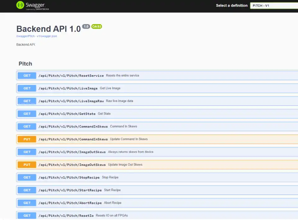
  • REST API service to integrate top-level test application to perform such functions as start/stop capture, start/stop generation, query system status (run, halt, errors), and perform loopback test.
  • User-editable JSON configuration files for image definition and bit streams, including channel skew adjustments.
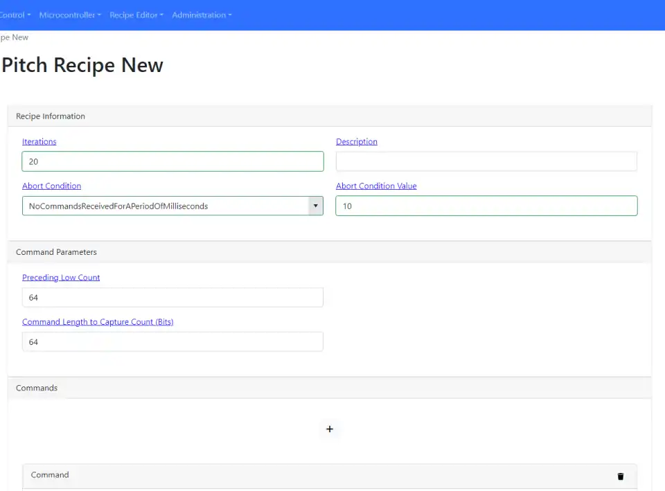
  • User-editable JSON recipe file to control test flow for unique and repeatable test runs.
  • RAID data storage for retrieval during generation and storage during capture.
  • Hardware abstraction layer – handles interface translation for various hardware interfaces, including, but not limited to NI FlexRIO, NI HS Serial, NI DAQmx, and NI R Series cards.
  • FPGA real-time processing, signal analysis, and signal generation with NI FlexRIO, including incorporation of proprietary VHDL into the FPGA.

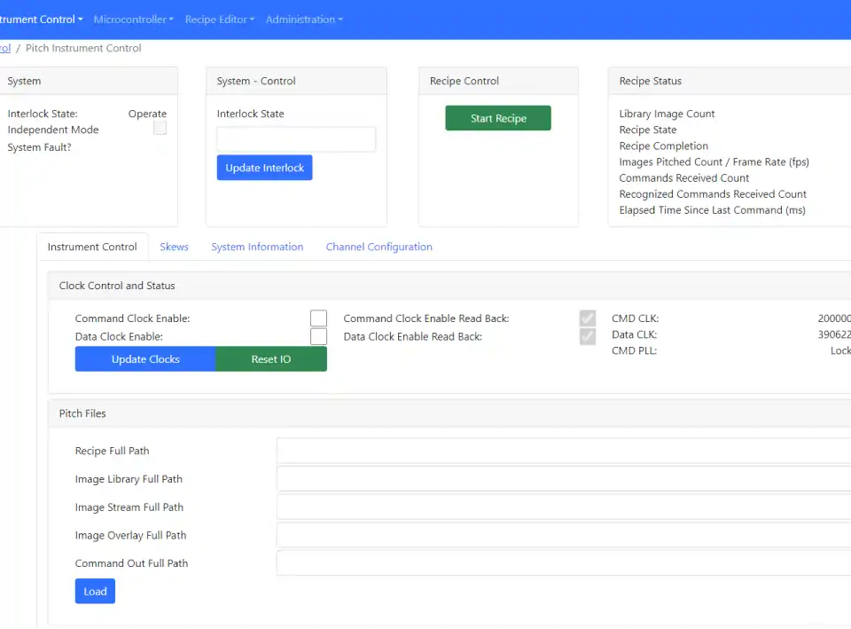
Below is a simple example application screen using LabVIEW to interface to the AEDIS platform.

Figure 1 - Sample simple test application screen

AEDIS Signal Conditioning I/O Features

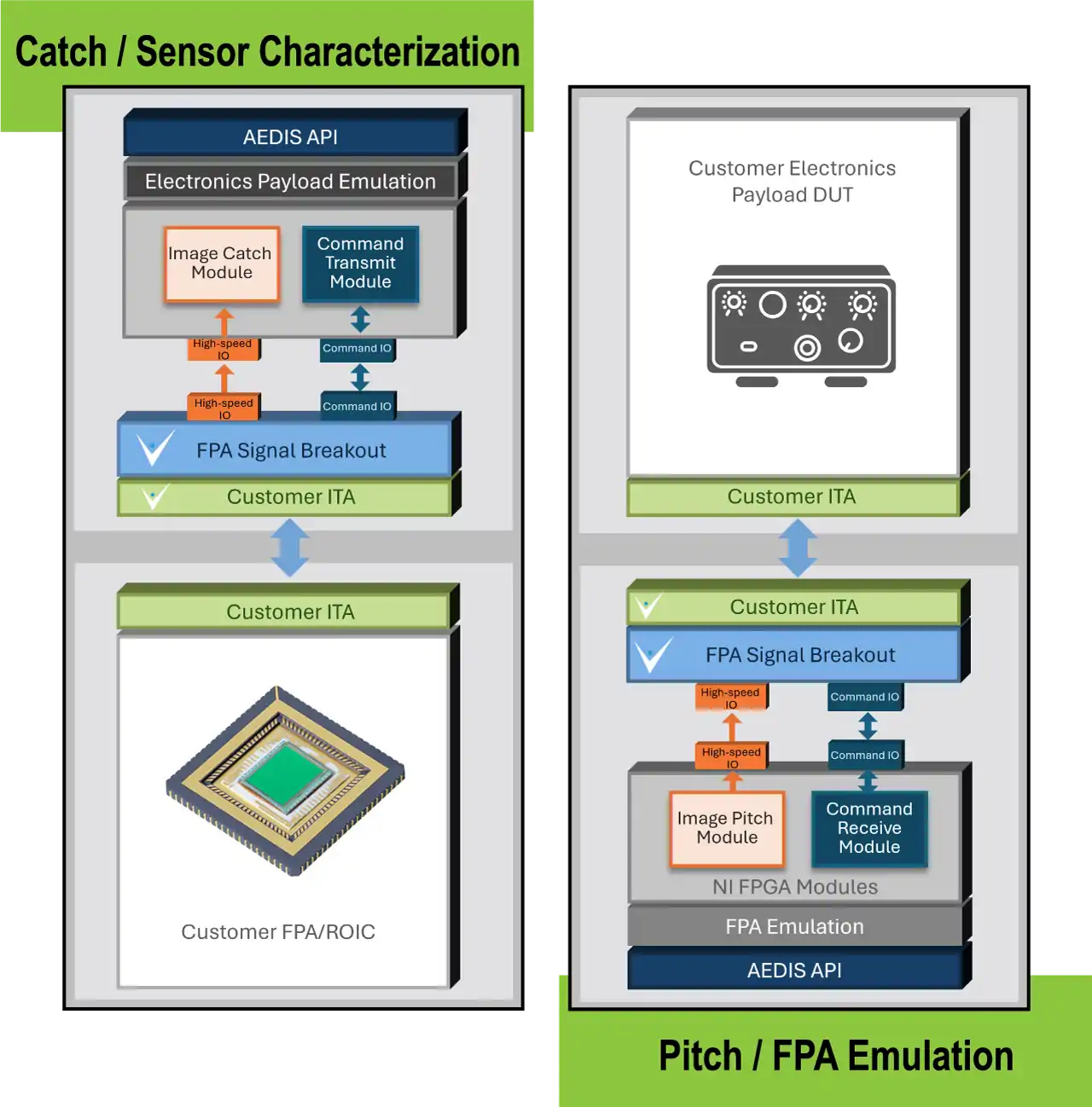
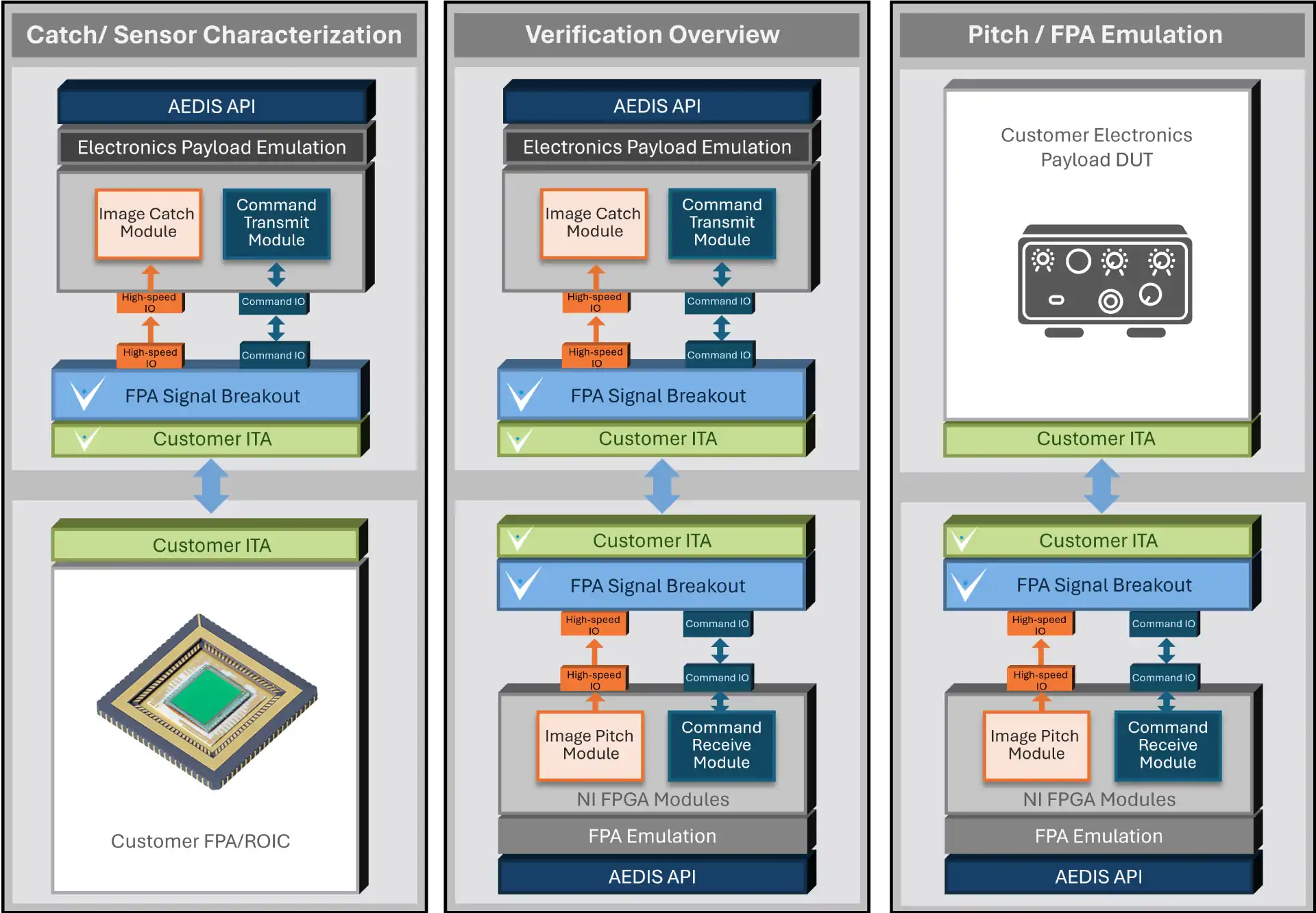
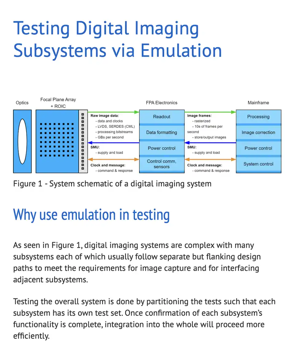
The AEDIS platform provides full functionality for baseline image pitch and image catch capabilities based on off-the-shelf PXIe hardware and AEDIS hardware connection (breakout ITA) interfaces.

Generally, your DUT’s signal I/O connects to the PXIe FPGA modules though buffer boards which connect directly to NI’s FlexRIO modules, generally PXIe-659x for SerDes/CML, PXIe-6569 for LVDS, and others as specifications dictate). These buffer boards mount into the AEDIS breakout ITA, providing quantity and type changes to accommodate the signal types used by the FPA and associated electronics.

  • High-speed FPA/ROIC and FPA electronics data path using LVDS and/or SerDes.
  • DUT Command interface support.
    • Clock and data command control driven by FPGAs.
    • SPI command / response message control.
  • FPGA I/O signals are buffered and buffer boards contain test points for probing and timing calibration.
  • Signal conditioning boards provide:
    • Power monitoring and DUT protection via an onboard µC.
    • Each channel buffer provides equalization and pre/de-emphasis with the setup controlled by a µC in communication with the AEDIS application.
    • LVDS rates up to 1.25 Gbps with up to 32 input and 32 output channels per module.
      • Per line programable transmit pre-emphasis and receive equalization.
    • CML has per line programable transmit pre-emphasis and receive equalization buffering with AC-coupled pairs with signaling rates to 6.25 Gbps per pair have been used with up to 4 input and 4 output channels per module.
      • Per line programable input equalization, output de-emphasis, differential voltage and slew rate limiting.
    • High-speed SEARAY™ connection to personality module.
  • Mates with NI FlexRIO PXIe-659x modules for SerDes/CML and PXIe-6569 for LVDS.
  • External synchronization.

The image below shows the AEDIS CML SerDes “FIM02” module. Test probes can be placed on this module to test signal integrity and timing.

Figure 2 - CML SerDes buffer I/O module

The image below the AEDIS LVDS “FIM03” module. Using the same connectors as CML SerDes module. Test probes can be placed on pads exposed on this module.

Figure 3 – LVDS buffer I/O module

AEDIS Breakout ITA Features

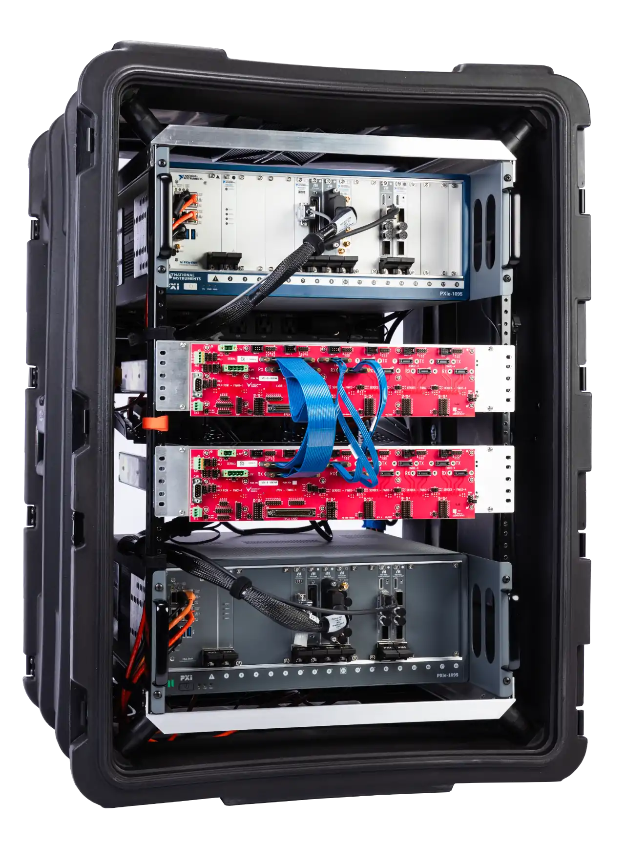
The AEDIS breakout ITA chassis is designed to hold up to 4 buffer boards along with a built-in power board to power the I/O buffer modules. The I/O module mix is configurable. The buffer I/O modules are connected to the high-speed ITA connectors via a PCB which provides the conversions to your DUT’s connectors and cables.

Other I/O schemes needing different channel types and counts and, especially, specific user connector types and counts, rely on the customizability of the PCB to make the connections. Often, the user wants a custom PCB so actual product (DUT) cables and connectors can directly connect to the AEDIS hardware.

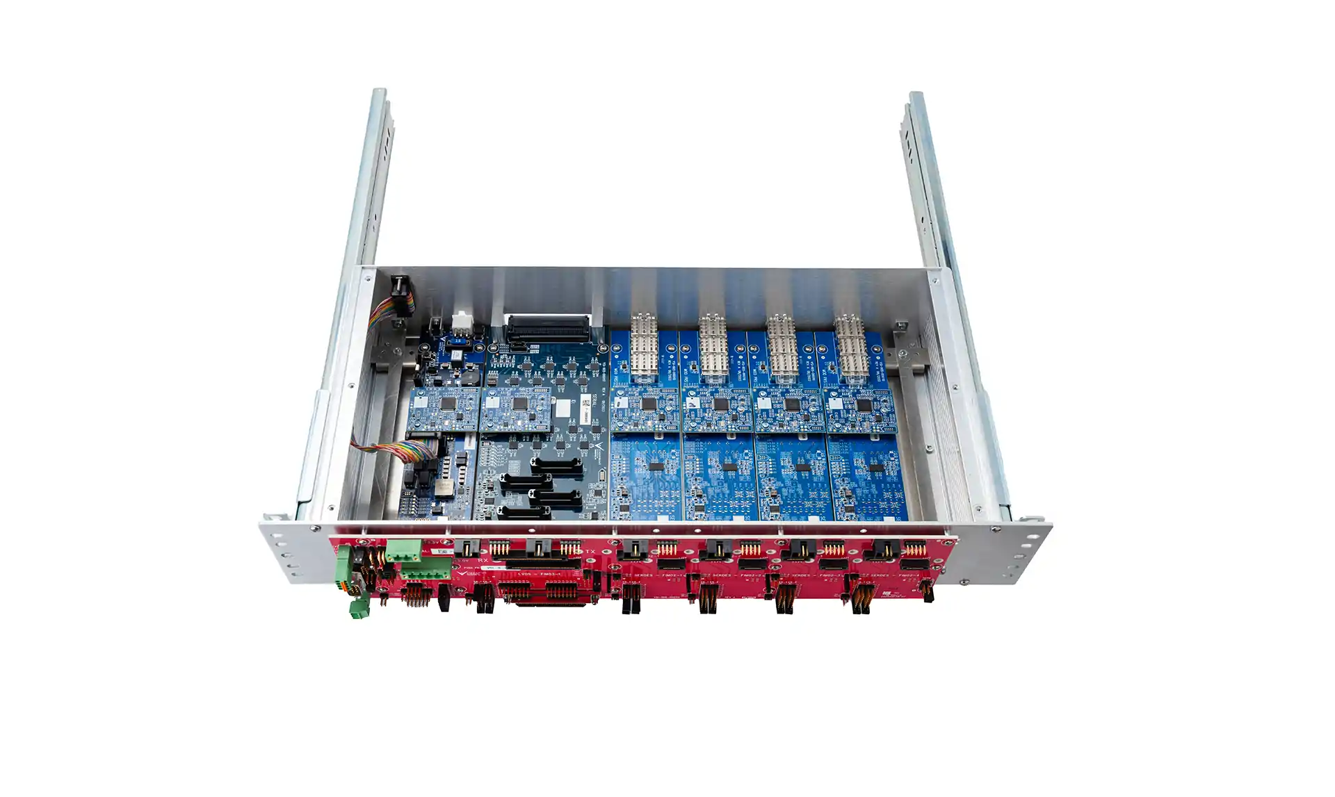
The image below shows a breakout with 16 SERDES pairs, 32 LVDS Inputs and outputs. Shown with two Airborne VerSI connectors.

Figure 4 - AEDIS breakout ITA (top and back panels removed for clarity)

Benefits

For many people, the AEDIS platform offers a complete design validation and manufacturing test system for designing and manufacturing the FPAs and associated electronics in their EO/IR imaging products. Customization is available for those that have unique needs.

AEDIS offers these high-level benefits and more:

  • Reduced schedule time and development cost
    • Core set of software components ready to use.
    • REST API to interface AEDIS to your test set
    • Pre-built buffer electronics and ITA work with NI FlexRIO hardware.
    • JSON file defines sensor size, interfaces, and IO count.
    • Unique recipe JSON file for controlling test flow.
  • Validation readiness
    • AEDIS pitch platforms can be validated by AEDIS catch platform and vice versa.
    • Loopback capable
    • I/O buffer hardware has test points to validate signal integrity and correctness.
  • Customization
    • Single PCB for configuring your specific interconnects and channel counts.
    • Extendable and modular hardware and software architecture.
    • JSON-based script to execute your specific test types.

We’ve found that AEDIS typically starts at about 80% complete for each customer system, since each customer brings unique needs related to the digital data channel connection schemes and combinations of data and clock details. Those unique needs usually require building configuration files and/or software customization that consumes less than 20% of the overall scope of the test system.

Want to chat?

Case Studies

Automated production test of EO/IR imaging subsystem

Automated production test of EO/IR imaging subsystem

Assessing quality of mission-critical electronics for imaging

Increased throughput by automated signal skew adjustment and pixel verification

Client – Worldwide supplier of products for aerospace and defense

Challenge

Our client wanted a test system that would significantly increase production rates for a very specialized focal plane array (FPA) and associated readout integrated circuit (ROIC) electronics.

In broad strokes, the system needed to support the following:

  • Increase production test throughput as much as reasonably possible within budget and schedule constraints.
  • Provide some low-code or no-code way to create new test protocols.
  • Protect the DUT using hardware and software interlocks.
  • Verify the correctness of test image(s) and all its pixels.

Solution

The FPA and ROIC testing for this client used many of the same techniques we have implemented for FPA/ROIC testers at some of our other clients. Thus, the solution was built around our AEDIS platform and some custom connectivity hardware which paired the DUT to the AEDIS hardware.

Specifically, the test needed to:

  • Send digital signals from the AEDIS hardware to initiate and coordinate the test steps.
  • De-skew bitstreams from the DUT.
  • Organize and rearrange the bitstreams into image pixels.
  • Provide custom “personality” modules to connect the DUT and AEDIS hardware.
  • Protect the DUT from connection and power faults.

Benefits

All the bulleted items above are common requests from our clients and are supplied with the AEDIS platform or easily accommodated by design of the platform. Consequently, AEDIS often meets 80% or even 90% of typical client needs.

Thus, the client was able to cost-justify an AEDIS-based solution for two main reasons:

  • overall system costs for an AEDIS-based solution were significantly less than a completely custom system and
  • the increased production rates provided plenty of schedule buyback.

Furthermore, the script-based, low-code capabilities offered by AEDIS enabled:

  • Support of different test images.
  • Control of image transfer initiation, handling responses from the DUT, and flow.
  • Version control (by the client) of script-based test configurations.
  • Defined parsing of bitstreams to create the image pixels to simplify downstream image collection.

System Overview

The test system was built around AEDIS, which is a combination of five major components:

  • NI FlexRIO PXI modules and chassis.
  • Signal conditioning hardware.
  • A REST API interface for the client’s test sequencer and LabVIEW FPGA for the hardware interfacing.
  • An out-of-the-box browser-based app to interact with the AEDIS system.
  • A source measure unit to supply and test the DUT’s power needs.

With this design, AEDIS acts as an instrument to incorporate into the client’s overall test system.

The NI FlexRIO modules use Xilinx FPGAs for digital I/O at the rates and channel counts required to fully test the FPA on the DUT. Some digital lines were used for commands to the FPA while most were used to receive output from the FPA.

The AEDIS interfacing hardware acts as an ITA while converting the FPA/ROIC signals to types expected by the FlexRIO. A custom “personality” module provides the physical connectivity from the client’s hardware cabling to the ITA. The AEDIS software handles the test configuration setup, data acquisition, and data storage via high-speed RAID drives.

During development of the test system, AEDIS hardware and software were also used to emulate the actual FPA and electronics to verify, before deployment, that the test system was working as required. This same setup can also be used for periodic verification as might be needed for an annual equipment performance audit.

Finally, configuration files were built from user-created scripts to give the client flexibility for adding new test capabilities for the DUT.

Some of the significant hardware and software challenges mitigated by this combination of PXI FlexRIO and AEDIS are:

  • Interface to tester: The AEDIS system is treated as an instrument managed by an overall test system. The client developed some custom C# code to interface to the AEDIS REST API interface to automate their test procedures.
  • DUT interfacing: Standard (keyed) cabling ran between the DUT and the custom AEDIS “personality” card to match cabling to the DUT. The output of this personality module went to the AEDIS LVDS modules.
  • Channel skew: The high-frequency digital LVDS signals from the DUT can develop noticeable timing skews between channels upon arrival at the FlexRIO inputs due to signal path length differences. The test system had to detect and accommodate for these skews before combining the bits streams into bytes, then pixels, then an image.
  • High data rates: Not only were the digital data output at high frequency but many channels were needed to accommodate the full frame rate of the DUT. The FPGA and the PXI backplane needed enough processing and transport bandwidth to accommodate the throughput.
  • Interlocks: Keyed cabling and “signal present” software checks assured proper connections between the DUT and the AEDIS hardware before testing would begin. These safety checks were justified due to the high cost of each DUT.
  • User-defined scripts: Scripts created and edited by the user provided flexibility to address future test types and system obsolescence. For example, the scripts defined details such as a) the DUT-specific commands (some of which could not be shared with us for secrecy reasons), b) when the image is being captured (or ignored), and c) if the image is stored to disk or RAM.
SOFTWARE FUNCTIONS
Browser-based app for manual operation and recipe creation and editing
REST API interface for support of automated operation
Configuration of the test via scripts
Pre-test interlock checks
Data collection, bit stream processing, and mapping digital bitstream to pixels
HARDWARE USED
Standard AEDIS components for signal buffering, conditioning, and signal acquisition
Custom personality hardware for connectivity and physical connection interlocks
Signal test points in AEDIS breakout ITA modules enabled use of a logic analyzer for troubleshooting and further verification

High-Speed Digital Subsystem Emulator

High-Speed Digital Subsystem Emulator

Client: A large company involved in C4ISR

At maximum throughput, the AEDIS systems needed to consume and produce more than about 800 MB/s/slot.

Background

A large company involved in C4ISR was developing a system for a new high-speed digital sensor device. Viewpoint was contracted to build a test system used in design validation and ultimately endurance testing of the sensor. Since the sensor was a component of a larger system which was being developed at the same time, another test system was created to simulate the sensor by feeding signals into the system. This ability to use HIL testing for both the sensor and the downstream sensor electronics enabled parallel development, thus saving time and reducing schedule.

Challenge

Both the amount of data and the frequencies of the various digital signals were nearly at the limit of hardware capabilities. At maximum throughput, the systems needed to consume during record and produce during playback about 800 MB/s/slot. The FPGA clock on the FlexRIO had to run up to 300 MHz. The skew between triggers for data transmission needed to be less than 5 ns even between multiple FlexRIO cards even when the parallel data paths have inherent skews associated with the sensor. Finally, the systems needed to handle clocks that might be out-of-phase.

Achieving these requirements required significant engineering design in the face of multiple possible roadblocks, any one of which could have eliminated a successful outcome.

Furthermore, as usual, the development timeline was tight. In this case, it was a very tight 3 months. Basing the solution on our AEDIS platform was critical to meeting this challenge.

Viewpoint’s Solution

To meet the timeline, we had to work in parallel across several fronts:

  • LabVIEW-based application development for both record and playback
  • LabVIEW FPGA development for marshalling data between the controller and DRAM
  • Custom FAM circuit board design and build
  • FlexRIO FPGA CLIP nodes and code for low-level data handling

Technical Highlights

This sensor had several parallel data paths of clock and data lines with clock speeds up to 300 MHz on each path requiring exacting design and build of a custom FlexRIO Adapter Module (FAM) and unique custom CLIP nodes for extending the FlexRIO FPGA capabilities. The FAM also had a special connector for interfacing to the customer’s hardware.

Additional NI hardware and software completed the system components.

Results

The choice to base the AEDIS emulators on NI hardware and software was critical to completing this project. The open architecture in both hardware (custom FAM) and software (CLIP Nodes) enabled us to include some very creative extensions to the base toolset without which the project would not have succeeded in the allotted pressured schedule and on a predetermined budget. We were able to stretch the capabilities of the hardware and software very close to their maximum specifications by combining COTS and custom much more cost effectively than a purely custom design. Further, with HIL tests, both the sensor and the sensor electronics could be developed in parallel, leading to a significant schedule buyback for our client.

LabVIEW Layers

The host application, written in LabVIEW, managed the configuration of the data acquisition and the control of the LabVIEW RT-based FlexRIO systems. The configuration primarily dealt with the number of sensor channels in use, skew settings between digital lines, and other parameters that dealt with the organization of the data passed between the sensor and the FlexRIO.

Two FlexRIO applications were written, one for record and one for playback. Each FlexRIO application was written in LabVIEW, and managed the configuration of the FlexRIO cards and the movement of data between the FlexRIO cards and the RAID drives. Note that Windows supported for the RAID driver. Between 10 and 32 DMA channels were used for streaming, depending on the number of sensor channels being used.

And, each FlexRIO application had an FPGA layer, written in LabVIEW FPGA enhanced with custom CLIP nodes. For the record application, we developed a custom DRAM FIFO on the FPGA to assist with the latencies on the PXIe bus. For the playback application, we were able to stream directly from DRAM.

FlexRIO Considerations

The FlexRIO and stock FAMs from NI were initially considered as candidates for this project. Clearly, working with commercial-off-the-shelf (COTS) components would be most effective. Three options were available at the project start which could accommodate the required clock frequencies, but none offered both the required channel counts and skew/routing limitations. Hence, we had to design a custom FAM. This decision, made before the start of the project, turned out to be wise in hindsight because the parallel development path resulted in some shifts of sensor requirements which could be accommodated with the custom FAM but might have led to a dead-end with a COTS FAM.

FlexRIO CLIP

In LabVIEW FPGA, a CLIP Node is a method to import custom FPGA IP (i.e., code) into a LabVIEW FPGA application. CLIP stands for Component-Level Intellectual Property. We needed to use special Socketed CLIP Nodes (i.e., VHDL that can access FPGA pins) for this project because we could expose additional features of the Xilinx Virtex-5 not exposed in LabVIEW FPGA by accessing Xilinx primitives. Some specific features were:

  • Faster FPGA clocking
  • Additional clocking options
  • Individual clock and skew control
  • Custom PLL de-jitter nodes

Essentially, the FPGA design had a majority of FPGA code developed in LabVIEW FPGA and we used CLIP Nodes for interfacing the signals between the FlexRIO and the FAM.

DRAP-case-study-image

FlexRIO Adapter Module

As mentioned earlier, we had to create a custom FAM because of the need to route high speed signals from customer-specific high density connectors while synchronizing signals across multiple data channels and FPGA modules to within one (300 MHz) clock cycle.

At these high-speeds, the FAM needed careful buffering and impedance matching both on the signals as well internal components on the FAM PCB. At the start of the design, we utilized Mentor Graphics HyperLynx High Speed DDR signaling Simulation software to minimize signal reflections prior to building actual hardware. This step saved countless hours in spinning physical hardware designs.

We designed the FAM to allow channel routing and access to additional clock and trigger pins on the Xilinx chip and PXIe backplane.

White Papers

Testing Digital Imaging Subsystems with Emulation

Testing Digital Imaging Subsystems via Emulation This article discusses an emulation platform built from COTS-based hardware for testing digital imaging systems. For a comprehensive coverage of typical tests, the main [...]

This website uses cookies and third party services. See our privacy policy for more info. OK