AEDIS
Emulation of high-speed
Digital Imaging Subsystems
Customizable integrated hardware and software platform to meet the needs of Focal Plane Array interface protocols
What is AEDIS?
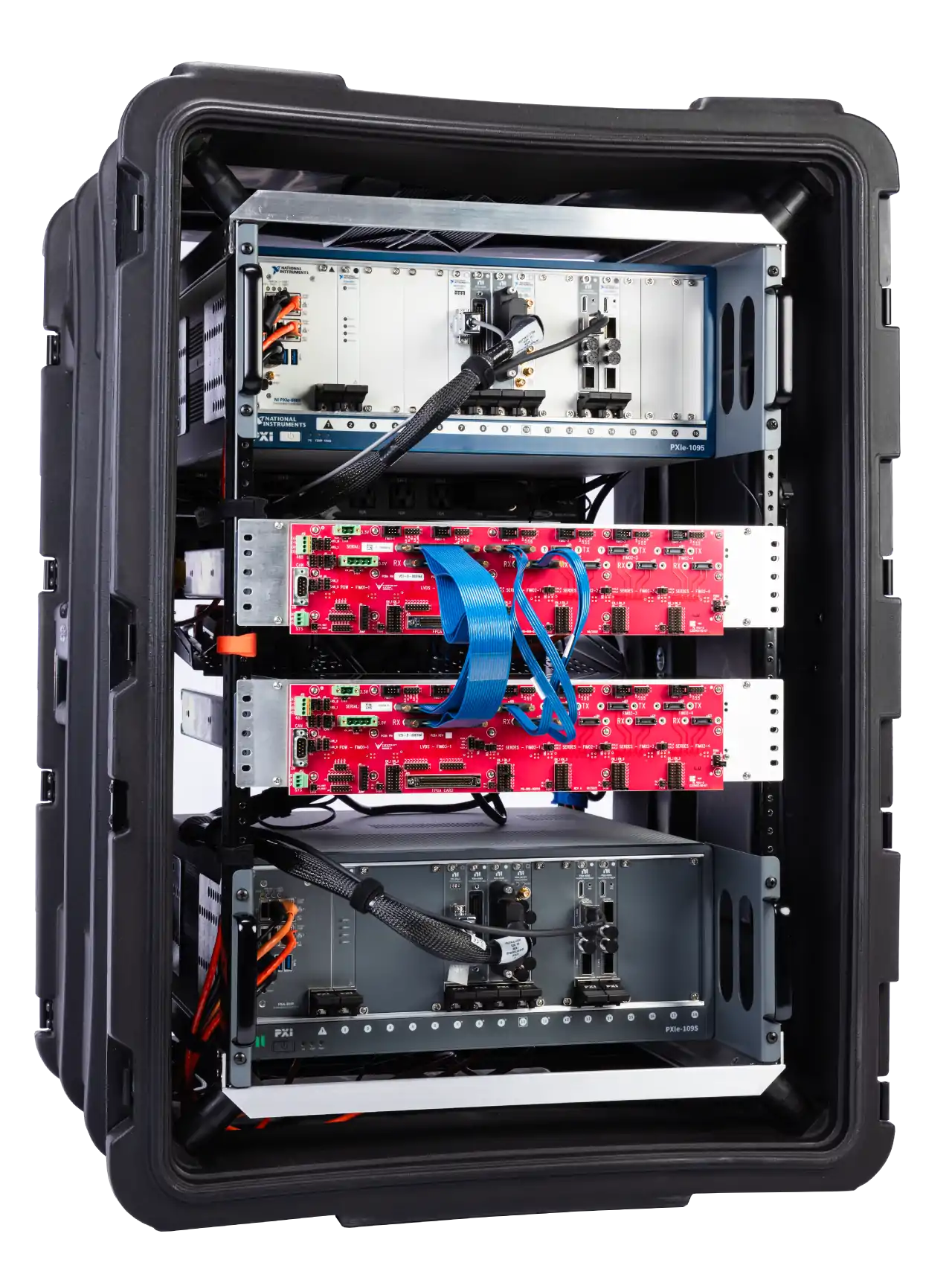
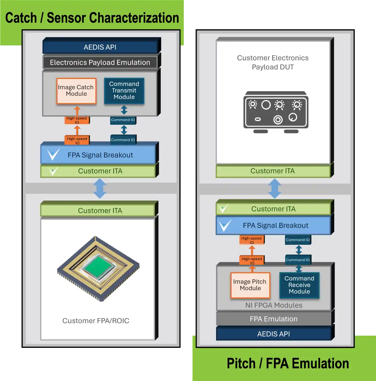
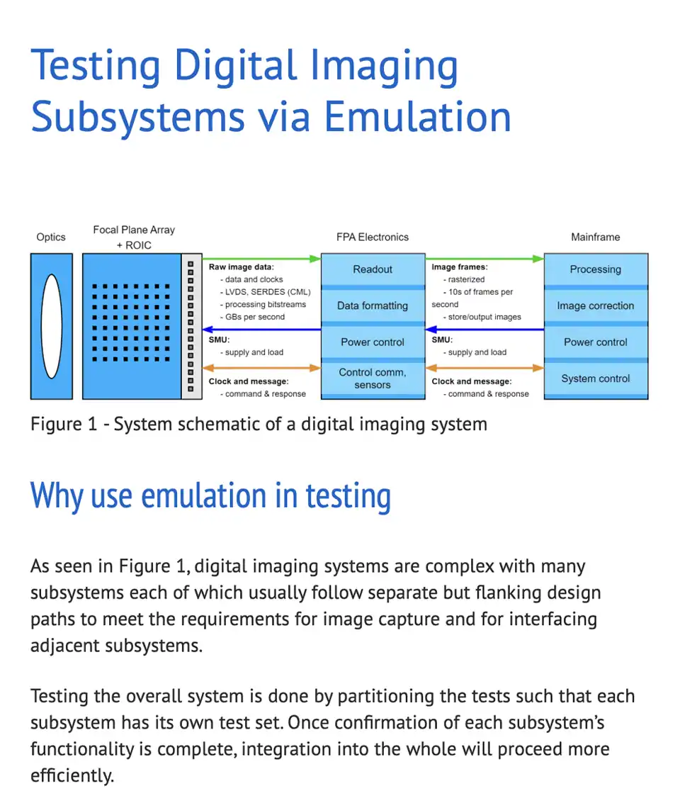
AEDIS is a platform instrument for testing Focal Plane Array (FPA) image sensors and/or the downstream interface electronics. It is a pre-built system of both hardware and software components to meet the needs of custom FPA interface protocols.
Built on NI’s FlexRIO and PXIe hardware, AEDIS satisfies 80% of common requirements for FPA and downstream electronics testing, vastly accelerating development times and significantly reducing risk compared to an in-house developed platform.
 Pre-built, 80% complete at start
- Client focused adaptable system
- Significantly cut development timelines
 Pre-built, 80% complete at start


Schedule Buyback
The software architecture leverages foundational core FPGA functionality coupled with templates to handle your exact protocol characteristics.
Handling your specific data flow, framing, and bit streams is a matter of modifying existing code templates, state machines, and configuration files. Your risk of schedule slippage is drastically reduced. Pre-built buffer electronics with modularization minimizes customization for specialized interconnects. Test points enable access for formal signal integrity analysis.
Data reduction options are available that decreases post-processing time.
Time & Risk Reduction
With the bulk of pre- or post-processing performed in the FPGAs, test engineers don’t need to process images just to fit some standard form. AEDIS accepts and produces in real-time the images in the same form as the FPA. With the log jam of raw test data gone, the pressure and risk of discovering that the test was invalid is removed.
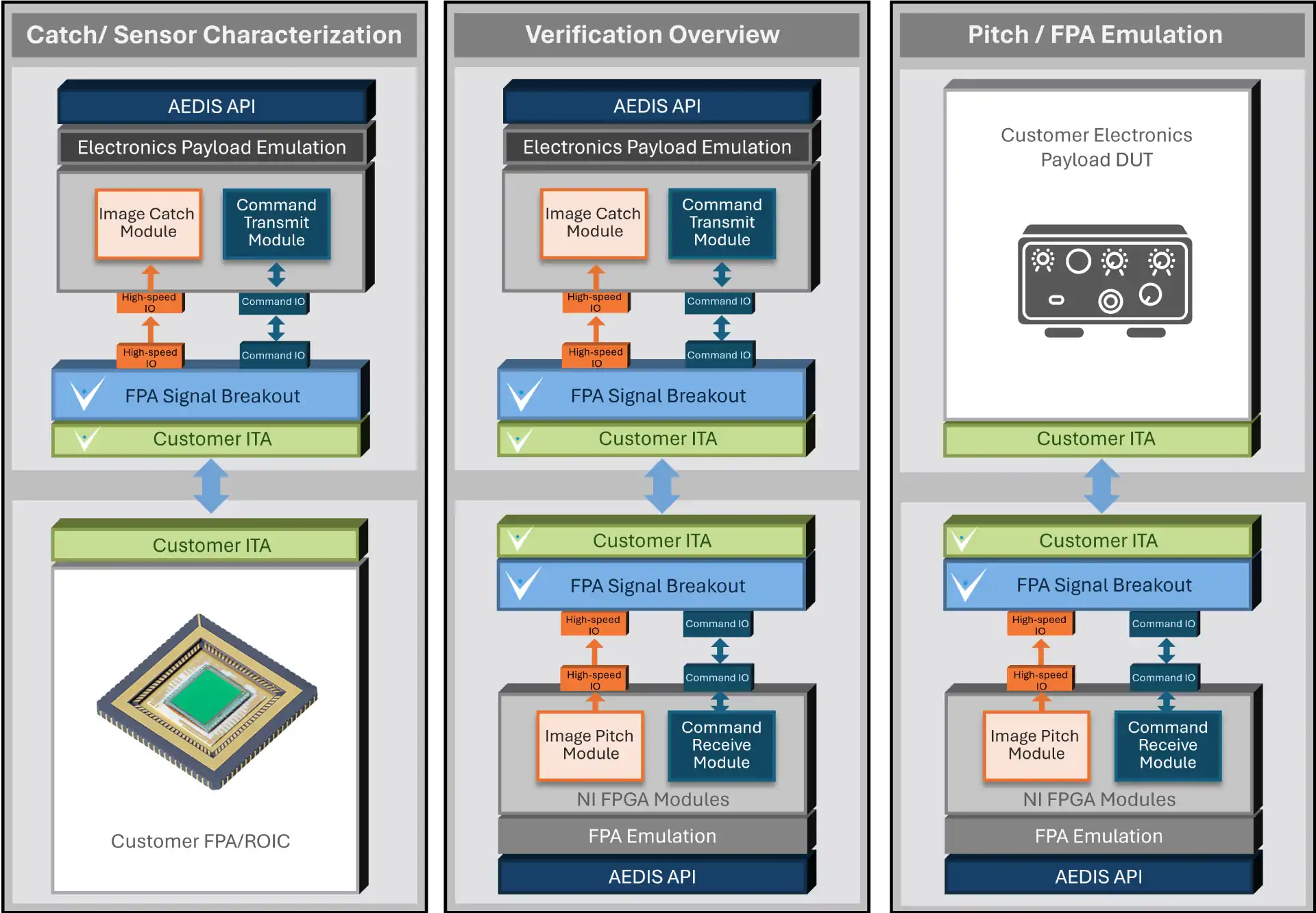
Verification of Delivered System
The AEDIS platform comes complete with all sides of the data and command interface. So, whether you're emulating the FPA or the Electronics interface, AEDIS has the complementing functions that allow for extensive verification before delivery to you.
Live Image
The AEDIS live image feature allows you in real time to the images going across the wire.
Setup and debug of a device under test is simplified with such immediate feedback.
Lifetime Advantage

Same Software
Interface
Software interface is interchangeable between various sensors.
The AEDIS API doesn’t need to change just because the sensor specifics have changed. The software tooling used to interface to the system can be reused for other sensors or programs.

Modular
Hardware
Hardware is modular to meet long term interface requirements and changes.
The NI and Viewpoint modular hardware allows new sensors/interfaces handled within the same architecture. The front‐end personality card is the only custom piece that may require change.

Technology
Advances
Technological advances can be integrated as available.
This technology is based upon modularity both in NI modules and our own breakout modules.
A principal design aspect of AEDIS is the modularity of the NI modules, our breakout modules, and the software components. As technology evolves, we can use newer modules and software tools with improved specs to upgrade the system and keep pace with the latest hardware and software.

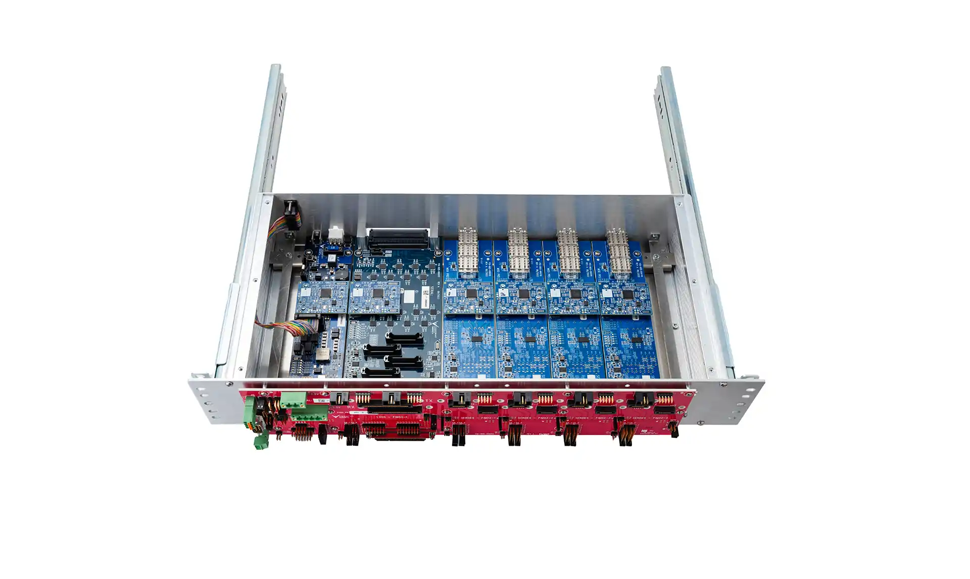
Hardware
- Modular pieces to directly connect to NI FlexRIO’s and modules
- May also connect to other ITAs
- Modules selected per application, other interface types may be available as well
- Modular electronics selected per application
- Scaled for many modules
- µC Controlled for current and voltage monitoring
- 32 channels in, 32 channels out
- Software configurable buffer control (per-channel)
- Test point access
- µC controlled with monitoring
- Wires all the I/O to customer chosen connector(s)
- Hi-speed interconnects to each module
- Additional I/O can be added
- High Speed Board to Module connections
- Interfaces to standard NI Cables
- Multiple Cards Supported
- SERDES/CML – 4 channels (bidirectional) per module, CML buffering
- Software configurable buffer control (per channel)
- Test point access
- µC controlled with monitoring
- Mil Style Connectors
- Mass ITA Connectors

System Configuration
Software Interfaces
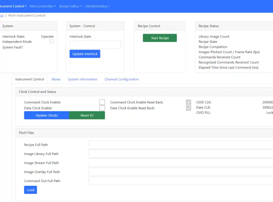
Allows system checking at start up without writing any software.
Instant feedback of issues saves days of setup and testing.
Can also be used for monitoring tests running from the API including live images.
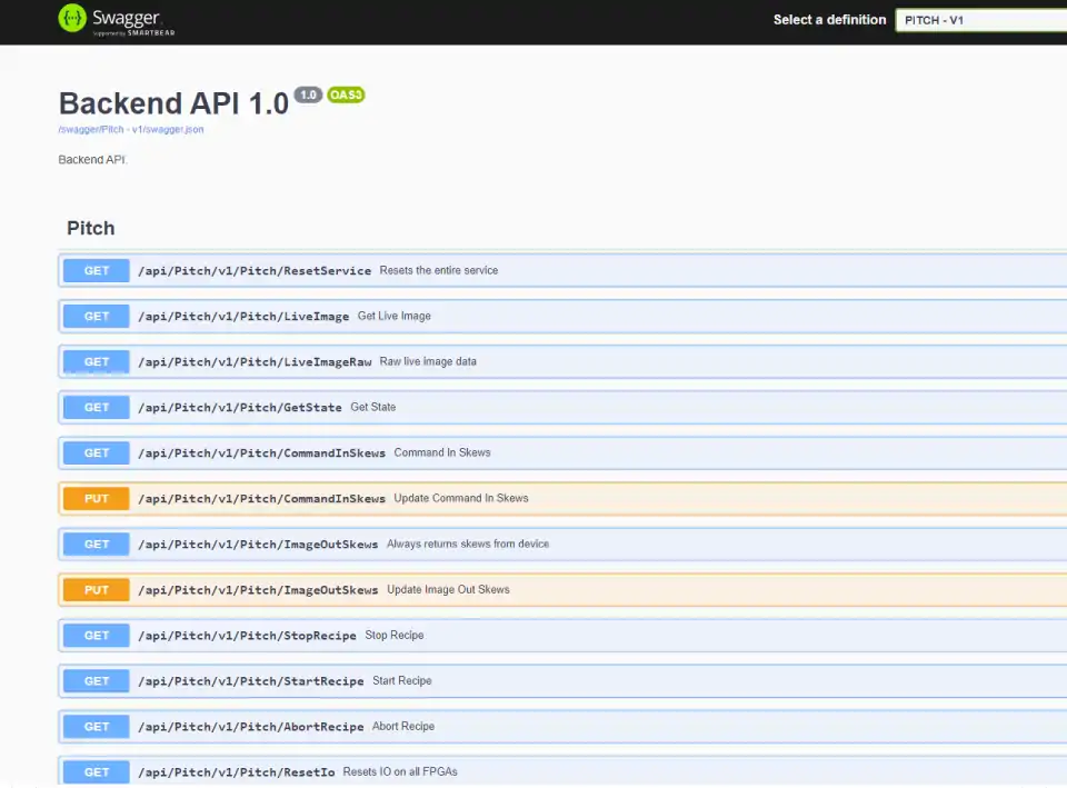
The API allows for accessing the AEDIS instrument via software control.
Major commands are: initialize, Reset, Configure, Change Interlock state, Start, Abort, Close
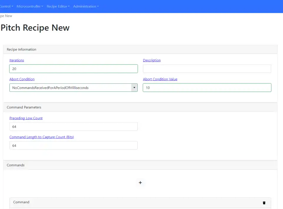
Recipes are the script-based, low-code capabilities offered by AEDIS. Recipes give you the capability of doing the following:
- Looping.
- Support of which of many test images to send out and when with accurate timing.
- Control of image transfer initiation
- handling responses from the DUT, and
- flow of commands and images.
White Papers
Testimonials
What customers are saying about AEDIS

Time Saving
“This will save us 3 man years of work in pre and post processing alone.”
– Program manager

Flexible
“I never thought we could have so much flexibility in image/data and really test at a complete system level.”
– Senior test engineer

Verification
“It is nice to know the system just worked when we received it, I can see why having the complementing system for verification really pays dividends.”
– Senior test engineer
