Test system development – sometimes custom electronics are better than COTS
When, why, and how we think about it
COTS products are great! There’s a reason they exist.

They:
And yet, in some situations, custom electronics can be a better fit for your test system.
The fundamental drivers for why custom make sense situationally are:
- Extra functionality – Custom often makes sense when the COTS components bring along more features than necessary. All those extra features cost more money, add points of failure, and can increase the difficulty in integration and maintenance of the test system.
- Performance limitations – Because COTS products are trying to meet the needs of so many scenarios, they may be limited for specific needs. add a microcontroller and an FPGA to some front-end custom electronics, and tasks difficult to perform in COTS can be made much easier. For example, using an FPGA to return timestamps of digital state changes across 100s of digital channels reduces data bandwidth that would otherwise be streamed across a PC bus.
- SWaP (Size, Weight, and Power) requirements – . A small, light-weight, and/or low-power test system may be preferred due to environmental constraints. For example, measurements made in a small chamber make I/O cabling difficult or the DUT moves during testing and a small, low-power wireless DAQ device can be mounted right on the DUT.
We’ve helped our clients identify custom test solutions that, because they are laser-focused on a particular testing need, can be cheaper, more easily deployed, or have higher performance than a COTS solution.
Custom is situationally preferrable to COTS for test because you can potentially:
- Save $ during development
- Save time during development
- Save $ in maintenance
- Improve reliability
- Improve performance
- Improve SWaP (Size, Weight, and Power)
How we identify opportunities for custom electronics
After we’ve engaged with our client and obtained a good understanding of the test needs, we start choosing the measurement and control hardware needed to execute the test plan. Those details include:
From this list, we start by looking for any sensors, such as thermocouples for temperature or accelerometers for vibration, followed by the equipment to digitize these signals. If control is needed, we do the same for output actuators.
For the complex measurements, we will decide if basic digitization of sensor output can be coupled with either sophisticated circuitry or compute capability via FPGA or microprocessor. This type of combination may replace several COTS components with lower cost, physical space, and power needs. For example, we can produce a “smart sensor” by measuring two analog inputs, correcting non-linearities, and then performing some calculations to produce a measurement of torque differential.
Then we look at how to connect it all together and how to power it.
During this process, we look to COTS hardware first. If we spot possible opportunities to save cost, reduce development time, increase reliability, or improve performance by going with a custom electronics approach, we’ll proceed to dig into the details. Of course, spotting these opportunities initially relies on some gut feel and experience where we sense that custom electronics might be a better solution. Many times, it’s not. But often enough the benefits are outstanding.
Below are some details about areas where we see these benefits.
Save $ during development
Examples of how:
- A custom PCB can be less expensive than complex harness configurations. Point to point connections still need to be made manually, but making a PCB is a lot cheaper than building an actual harness.
- A microcontroller or an NI sbRIO can reduce system cost compared to an expensive PXI card of which only a few channels or a small subset of features is needed.
- A custom front-end to a COTS NI cSeries card can be less expensive than a set of COTS signal conditioning modules and offer better field connectivity.
Save time during development
Examples of how:
- Modular pre-designed subassemblies can be combined for quick turnaround. For example, common blocks like power regulation, A/D, D/A, DIO, and so on can be plucked from a schematic library and incorporated quickly into a new custom design.
Save $ in maintenance
Examples of how:
- Custom PCBs are more reliable than custom cable harnesses and can be less expensive to build.
- Circuitry can be added to allow software access to hardware parameters and calibrations to simplify validation and calibration.
Improve reliability
Examples of how:
- Custom PCBs can be more reliable than custom cable harnesses.
- Custom PCBs or microcontroller-based subsystem can reduce system part count and hence reduce the number of failure modes.
- PCBs can control impedances of signals, giving better signal integrity.
Improve performance
Examples of how:
- A COTS solution doesn’t exist, e.g., a fast 28 VDC digital input module
- A custom front-end can improve precision by boosting signal-to-noise
- Remote, high-performance, critical circuitry can deliver the desired signal types without relying on expensive long-distance sensor or actuator cabling.
Want to see some case studies where custom electronics were leveraged for test systems?
Replacing Wire-wrap Boards with Software, FPGAs, and Custom Signal Conditioning
Replacing Wire-wrap Boards with Software, FPGAs, and Custom Signal Conditioning
Electronic components of fielded systems were aging out
Reverse engineering effort converted wire wrap boards to FPGA-based I/O
Client – Amentum – A supplier for Military Range System Support
Challenge
Amentum (www.amentum.com) supports a decades-old system deployed in the early 1980s. While the mechanical subsystems were still functioning, the wire-wrapped discrete logic and analog circuitry was having intermittent problems.
Systems designed and built decades ago can sometimes have wonderful documentation packets. Nevertheless, we’ve been burned too often when the docs don’t incorporate the latest redlines, last-minute changes, or other updates.
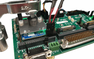
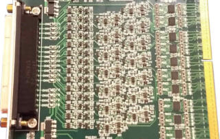
The replacement system needed to be a form-fit-function replacement to land in the same mounting locations as the original equipment with the same behavior and connections. Below is an image of the existing wire-wrap boards and their enclosure. We had to fit the new equipment in this same spot.
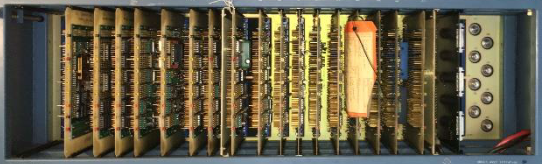
Figure 1 – Original wire-wrap boards
Finally, Amentum wanted to work with Viewpoint in a joint development approach. While our joint capabilities looked complementary, we didn’t know at the start how well we would mesh with our technical expertise and work culture – it turns out we worked extremely well together as a team and neither one alone could have easily delivered the solution.
Solution
Since the team treated the existing documentation package with suspicion, we adopted a “trust but verify” approach. We would use the documents to give overall direction, but we would need details from the signals to verify operation.
Leveraging Amentum’s experience with the fielded systems, the team decided early on to record actual signals to understand the real I/O behavior. We used the system’s “test verification” unit to run the system through some check out procedures normally run prior to system usage. This verification unit enabled us to use a logic analyzer for the I/O to and from the discrete logic digital signals and an oscilloscope and DMM for the analog signals. The available schematics were reviewed to assure that the signals made sense.
With a trustable understanding of system operation, Amentum created a requirements document. We jointly worked on the design of the new system. There were both an “inside” system (in a control shelter) and an “outside” system (in the unit’s pedestal).
Some overall tasks were:
- Viewpoint recommended an architecture for the inside application running on PXIe LabVIEW RT and FPGA layers.
- Amentum created the system control software on a Linux PC.
- Viewpoint developed the more intricate parts of the inside application and mentored Amentum on other parts they developed. This work recreated the existing discrete logic and analog I/O using PXIe NI FPGA boards.
- Viewpoint designed custom interposer boards to connect harnesses to the NI PXIe equipment, including a test point and backplane boards.
- Amentum designed and developed the cRIO-based outside system application and Viewpoint created a set of custom interposer boards to connect harnesses to the cSeries modules.
Critical to this project was our hardware selection services. By combining our engineering skills for the reverse engineering of the legacy electronics with our knowledge of the NI hardware, we narrowed the hardware choices to a few NI FPGA boards.
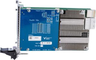
These PXIe FPGA boards and cRIO FPGA-backed modules handled the required 60 MHz clock-derived signals with correct phases, polarity, analog inputs, and so on. Furthermore, the wire-wrap boards were register-based so the PXIe had to decode “bus signals” sent over a Thunderbolt bus to emulate the programming and readouts from the various wire-wrap boards.
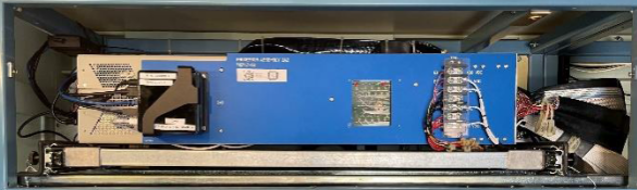
Figure 2 – PXIe replacement to wire-wrap boards
Amentum wanted to be able to support the LabVIEW FPGA VIs used to replace the functionality of the discrete logic. So, Viewpoint acted as mentor and code reviewer with Amentum to ramp them up on using LabVIEW FPGA effectively. Neither one of us alone would have been successful coding the applications in the allotted time. Joint knowledge and experience from both Viewpoint and Amentum were required.
Signal conditioning and harnesses needed to be reworked or replaced as well, of course, since the landing points for the wires were different in the new system. Viewpoint suggested a technique, which we’ve used frequently in past obsolescence upgrade projects, to create PCB boards that accepted existing connectors.
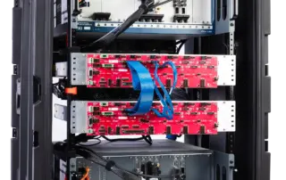
For the cRIO, these interposer “connection” PCBs plugged directly into the cRIO cSeries module. For the PXIe, these interposer PCBs accepted the field wiring connectors and converted them to COTS cables that connected to the PXIe modules. These interposer PCBs could have signal conditioning incorporated as needed. This approach significantly reduced the need for custom harnesses. All told, about 200 signals were passed between the PXIe and various other subsystems, and about 100 for the cRIO. This approach saved significant wiring labor and cost.
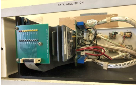
Figure 3 – cRIO with interposer boards between cSeries and field harnesses
The work to design and build the signal conditioning custom electronics was split between Viewpoint and Amentum. Viewpoint did more design than build and handed over the schematics and Gerber files to Amentum so they could manage the builds while also being able to make modifications to the boards as needed.
Benefits
Amentum wanted an engineering firm that was willing to work along side them as a partner. Joint discussions about architecture and design led to a collaborative development effort where Amentum benefited from Viewpoint’s extensive expertise and guidance on LabVIEW architectural implementation and FPGA coding style.
The main outcomes were:
- As a partner of the team, Viewpoint acted as staff augmentation by providing experienced engineers with technical capabilities that Amentum initially lacked.
- This team approach delivered a stronger product to the end-customer more quickly than either of us could do alone.
- The combination of Viewpoint’s and Amentum’s experience reduced the amount of reverse engineering needed due to the lack of firm requirements.
- Reduction of electronics obsolescence by using software-centric FPGA-based functionality. Recompiled LabVIEW FPGA could target future boards models.
- Increased software-based functionality simplifies future updates and modifications.
- Decrease in number of parts leading to simpler maintenance.
- Lower wattage consumed eliminated need for an anticipated HVAC upgrade.
- Cybersecurity concerns were reduced by using Linux-based systems and FPGA coding.
System Overview
Using software to emulate the old hardware was a critical success factor. Since the requirements were not 100% solid at the start of the project, some field-testing was required for final verification and validation. The flexibility of the software approach eased modifications and tweaks as development progressed. A hardware-only solution would have necessitated difficult and costly changes. For example, some of the changes occurred very near the final deployment after the system was finally connected to an actual unit in the field.
| SOFTWARE FUNCTIONS |
|---|
| Emulate original discrete logic functions via FPGAs |
| Emulate original analog signal I/O |
| Overall system control via Linux PC |
| Maintain the same user experience as existed before |
| Modern application architecture for simpler maintenance |
| HARDWARE USED |
|---|
| NI cRIO chassis with various cSeries modules |
| NI PXIe chassis with FPGA modules to handle all the analog and digital I/O via a combination of multifunction and digital-only cards |
| Custom PCBs for signal conditioning and connectivity |
Custom FlexRIO Adaptor Module supports HIL Test Upgrade
Custom FlexRIO Adaptor Module supports HIL Test Upgrade
A custom-COTS approach reduces cost and delivery time.
Client – Major National Research Lab

Challenge
Our client has a client (the end-user) for which they developed an HIL test system several years prior. Parts were obsolete and the system needed an upgrade. The prior system had many custom-designed electronic components which could not be replaced without a complete redesign.
Consequently, our client wanted to use COTS. However, one device needed 28 VDC digital I/O, a couple of lines which carried significant current (amp, not milliamp, levels) and at switching rates much higher than a COTS solid state relay could provide.
Solution
Viewpoint reviewed the requirements and created a hybrid COTS-custom solution. We combined an NI FlexRIO module with a custom FlexRIO Adapter Module (FAM) for the front end to satisfy the 28 VDC signals levels and required current drive.
Benefits
- COTS FlexRIO integrates into the remainder of our client’s PXI-based test system.
- The Custom I/O was designed for flexibility. Our client can use this FAM for both their initial end-user and other programs / clients too.
- Reduced cost relative to a completely custom solution.
- Delivery time reduced by months relative to a custom solution
FAM Overview
The custom FAM interfaced with the NI FlexRIO module, which offered low-level digital I/O (3.3 V logic), to digital signal conditioning hardware that provided the 28 VDC signal levels and required current drive.
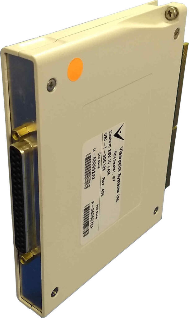
Each I/O pin was configurable as input or output (source or sink). Each bank of 4 channels had an adjustable threshold level set via an adjustable DAC output. Some of the channels are designed for amp-level current drive, while the remainder were 250 mA. All I/O was fused appropriately.
Viewpoint also developed LabVIEW FPGA and VHDL to enable our client and the end-user to:
- Configure the I/O as in or out.
- Communicate to the DAC to allow custom input threshold trigger levels.
- Read and write the digital data.
| SOFTWARE FUNCTIONS |
|---|
| Set the direction of each of the DIO channels |
| Set the threshold level on the input channels |
| Read / Write DIO Data |
| End User Application |
| HARDWARE UTILIZED |
|---|
| COTS NI FlexRIO |
| Custom FlexRIO Adaptor Module(FAM) |
| INTERFACES / PROTOCOLS |
|---|
| Customized VHDL Component Level Intellectual Property (CLIP) integrated with LabVIEW FPGA |
| LabVIEW FPGA as required along with LabVIEW and TestStand |
High-Speed Digital Subsystem Emulator
High-Speed Digital Subsystem Emulator
Client: A large company involved in C4ISR
At maximum throughput, the AEDIS systems needed to consume and produce more than about 800 MB/s/slot.
Background
A large company involved in C4ISR was developing a system for a new high-speed digital sensor device. Viewpoint was contracted to build a test system used in design validation and ultimately endurance testing of the sensor. Since the sensor was a component of a larger system which was being developed at the same time, another test system was created to simulate the sensor by feeding signals into the system. This ability to use HIL testing for both the sensor and the downstream sensor electronics enabled parallel development, thus saving time and reducing schedule.
Challenge
Both the amount of data and the frequencies of the various digital signals were nearly at the limit of hardware capabilities. At maximum throughput, the systems needed to consume during record and produce during playback about 800 MB/s/slot. The FPGA clock on the FlexRIO had to run up to 300 MHz. The skew between triggers for data transmission needed to be less than 5 ns even between multiple FlexRIO cards even when the parallel data paths have inherent skews associated with the sensor. Finally, the systems needed to handle clocks that might be out-of-phase.
Achieving these requirements required significant engineering design in the face of multiple possible roadblocks, any one of which could have eliminated a successful outcome.
Furthermore, as usual, the development timeline was tight. In this case, it was a very tight 3 months. Basing the solution on our AEDIS platform was critical to meeting this challenge.
Viewpoint’s Solution
To meet the timeline, we had to work in parallel across several fronts:
- LabVIEW-based application development for both record and playback
- LabVIEW FPGA development for marshalling data between the controller and DRAM
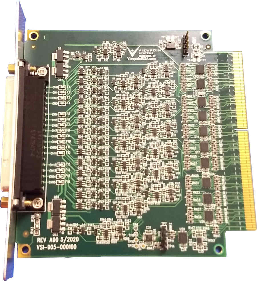
- Custom FAM circuit board design and build
- FlexRIO FPGA CLIP nodes and code for low-level data handling
Technical Highlights
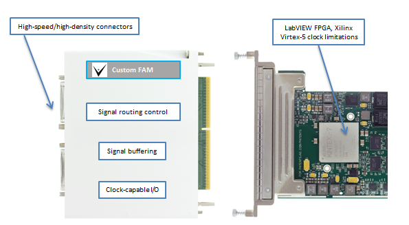
This sensor had several parallel data paths of clock and data lines with clock speeds up to 300 MHz on each path requiring exacting design and build of a custom FlexRIO Adapter Module (FAM) and unique custom CLIP nodes for extending the FlexRIO FPGA capabilities. The FAM also had a special connector for interfacing to the customer’s hardware.
Additional NI hardware and software completed the system components.
Results
The choice to base the AEDIS emulators on NI hardware and software was critical to completing this project. The open architecture in both hardware (custom FAM) and software (CLIP Nodes) enabled us to include some very creative extensions to the base toolset without which the project would not have succeeded in the allotted pressured schedule and on a predetermined budget. We were able to stretch the capabilities of the hardware and software very close to their maximum specifications by combining COTS and custom much more cost effectively than a purely custom design. Further, with HIL tests, both the sensor and the sensor electronics could be developed in parallel, leading to a significant schedule buyback for our client.
LabVIEW Layers
The host application, written in LabVIEW, managed the configuration of the data acquisition and the control of the LabVIEW RT-based FlexRIO systems. The configuration primarily dealt with the number of sensor channels in use, skew settings between digital lines, and other parameters that dealt with the organization of the data passed between the sensor and the FlexRIO.
Two FlexRIO applications were written, one for record and one for playback. Each FlexRIO application was written in LabVIEW, and managed the configuration of the FlexRIO cards and the movement of data between the FlexRIO cards and the RAID drives. Note that Windows supported for the RAID driver. Between 10 and 32 DMA channels were used for streaming, depending on the number of sensor channels being used.
And, each FlexRIO application had an FPGA layer, written in LabVIEW FPGA enhanced with custom CLIP nodes. For the record application, we developed a custom DRAM FIFO on the FPGA to assist with the latencies on the PXIe bus. For the playback application, we were able to stream directly from DRAM.
FlexRIO Considerations
The FlexRIO and stock FAMs from NI were initially considered as candidates for this project. Clearly, working with commercial-off-the-shelf (COTS) components would be most effective. Three options were available at the project start which could accommodate the required clock frequencies, but none offered both the required channel counts and skew/routing limitations. Hence, we had to design a custom FAM. This decision, made before the start of the project, turned out to be wise in hindsight because the parallel development path resulted in some shifts of sensor requirements which could be accommodated with the custom FAM but might have led to a dead-end with a COTS FAM.
FlexRIO CLIP
In LabVIEW FPGA, a CLIP Node is a method to import custom FPGA IP (i.e., code) into a LabVIEW FPGA application. CLIP stands for Component-Level Intellectual Property. We needed to use special Socketed CLIP Nodes (i.e., VHDL that can access FPGA pins) for this project because we could expose additional features of the Xilinx Virtex-5 not exposed in LabVIEW FPGA by accessing Xilinx primitives. Some specific features were:
- Faster FPGA clocking
- Additional clocking options
- Individual clock and skew control
- Custom PLL de-jitter nodes
Essentially, the FPGA design had a majority of FPGA code developed in LabVIEW FPGA and we used CLIP Nodes for interfacing the signals between the FlexRIO and the FAM.
FlexRIO Adapter Module
As mentioned earlier, we had to create a custom FAM because of the need to route high speed signals from customer-specific high density connectors while synchronizing signals across multiple data channels and FPGA modules to within one (300 MHz) clock cycle.
At these high-speeds, the FAM needed careful buffering and impedance matching both on the signals as well internal components on the FAM PCB. At the start of the design, we utilized Mentor Graphics HyperLynx High Speed DDR signaling Simulation software to minimize signal reflections prior to building actual hardware. This step saved countless hours in spinning physical hardware designs.
We designed the FAM to allow channel routing and access to additional clock and trigger pins on the Xilinx chip and PXIe backplane.
Next steps
Want to see if custom electronics makes sense for your automated testing needs?
Reach out here to see how we can help:
COTS products are great. In fact, during test system design and hardware selection, we look to COTS component first to take advantage of and leverage them whenever it makes sense. If you need help selecting NI-based test hardware, check out our NI hardware selection services and reach out if you’d like help. If we see a situation where a custom solution will be better suited and as or less expensive than COTS, we’ll want to discuss with you about pros and cons of using custom electronics for test.