
FPGA Gotchas: Four of the top 11 gotchas when developing with an FPGA
If you’re just getting started with or are considering utilizing an FPGA on your next project, as with anything complex, you realize you don’t even know what you don’t know.
We recently wrote a white paper on the top 11 gotchas when developing with an FPGA. Here’s a few of my favorites to get you started.
Gotcha #1: Thinking that you’re writing software
Get out of the software mindset – You’re not writing software.
Let me say that again because this is the single most important point if you’re working with FPGAs. You-are-NOT-writing-software. You’re designing a digital circuit. You’re using code to tell the chip how to configure itself. Now, before someone says it, yes, when you’re coding up one of the microprocessor cores within the FPGA, then of course you’re writing software, but that’s not what we’re talking about here. We’re talking about when you’re coding the digital logic.
Gotcha #9: Trying to use all of the FPGA!
In general, you want to use less than 100% of the part. The amount that you’ll want to keep in reserve depends on several factors, with significant factors including:
- The generation/architecture of FPGA being utilized
- Your code quality
- The FPGA clock rate
The fuller your part is, the longer the build process (compile, synthesis, place, route, etc.) will take. The reason this is a useful note, is that build times generally don’t take seconds. Depending on many factors, they can take 20 minutes, or four hours. In some cases it may fail to build at all, or worse yet, build, but be unstable, wasting countless hours in the lab.
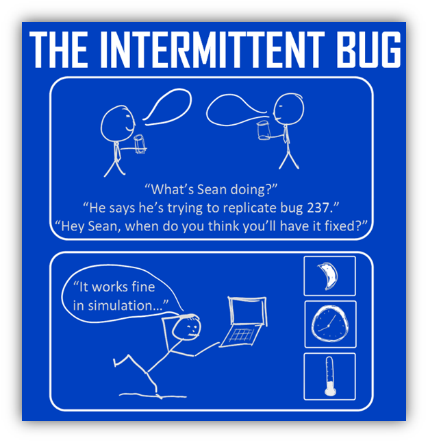
Gotcha #10: Not planning for Enough Bugs
Something about that feels wrong on first read, because who actually plans for bugs? You should. If you do it will be one of the most stress-relieving things you do, and you’ll thank me later. You’ll get many of the most basic level 1 bugs out during simulation, but at some point there will be a driving reason where you’ll have to move out to the lab and integrate your part of the world with the rest of the system being developed. This is where those famous words “But it worked fine in simulation…” come into play.
The disadvantage of a run-of-the-mill basic sequential processor is that only one operation is executing at any point in time. The advantage of a sequential processor is that only one operation is executing at any point in time. When it comes to debugging, the sequential nature of the basic processor makes life easier than debugging the parallel nature of the FPGA. While the simulation environment offered impressive visibility, now that you’re moving into hardware, your visibility into what’s going on decreases significantly.
Plan for a lot of bugs. Take a couple hours and think through other bugs you’ve dealt with as an engineer. Now triple that number (I’m making this multiplier up of course). If you’re a newbie developer, you need to pull in someone that has experience with FPGA development to help with this estimate. You’ll be wrong, but you’ll be better off than if you hadn’t thought this through. Here are a few tips on debugging to help you along the way: Six debugging techniques for embedded system development.
Intermittent bugs are common within FPGAs. They can be affected by temperature, humidity, the phase of the moon (I may be exaggerating a bit there, but sometimes I wonder).
The logic analyzer is your eyes into the inner workings of the FPGA. You can view outputs of course, and you can create test points to go to a testpoint header, but you have to be able to probe all of those points, so you’ll probably need a logic analyzer, which can get very pricey (if you’re looking for an inexpensive logic analyzer, check this out: https://www.saleae.com/ , and similar). A logic analyzer is a very important tool for FPGA-based development.
An internal logic analyzer can be helpful as well, at least in some scenarios. You may be able to get away with embedding test resources into your device (e.g. Xilinx has the Integrated Logic Analyzer), but this will utilize FPGA logic and memory resources, and is often challenging to see enough breadth or depth about what’s going on inside your FPGA. However, generally these tools are better for augmenting a true logic analyzer, as opposed to replacing them outright.
Gotcha #11: Making fun of the software guy!
The software guy (or girl of course; the term “guy” is used here androgynously) is your best friend – If your FPGA interfaces to a higher level supervisory sort of processor and/or it provides the UI, the software guy can do things to help make your life a lot easier. A couple of the more major categories include:
- Engineering debug panels – chances are the information you need to view is not the same as what the end-user needs to view. Having a debug panel can save you significant time, effort, and frustration.
- Special debug functions and modes – maybe there is some routine that software normally runs through with steps 1-12, but maybe you want to be able to run just step 3 and 4 repeatedly, or maybe just step 7 once. Or perhaps software can add a special function to keep track of the content or frequency of messages that you’re sending to it and set a trigger when something unexpected happens.
Work with the software developer early on to see how you can work together to facilitate the integration and debug process, and remember that it goes both ways. Chances are there is additional functionality that you could add to aid in their debug process as well.
Next Steps:
If you like these gotchas and want to see the others, read the white paper here:

David LaVine
David was the Marketing Manager & Solutions Architect at Viewpoint. David has a BS in Electrical Engineering from Rensselaer Polytechnic Institute and an MS in Electrical and Computer Engineering from Georgia Tech. He worked at Viewpoint Systems from 2013 – 2019.