
HDL FPGA Development –
The Good, the Bad, and the Ugly
Let’s talk about where FPGAs are today, where they were just a few years ago, and some pain points that still exist
Intro
Each year the various journals and publishers of embedded systems design material are seeing more and more talk of field-programmable gate arrays (FPGAs). FPGA technology is often talked about as one of the most powerful, but also one of the most frustrating parts of the embedded designer’s arsenal. With each generation of FPGA technology being faster, having smaller geometry and lower power, and with more logic gates, all for less money per operation, the possibilities seem endless. However, with great power (and re-configurability) comes, at least with FPGAs, some serious learning curves and frustrating days (weeks) at the office. Let’s talk about where FPGAs are today, where they were just a few years ago, and some pain points that still exist.
The Good
Large, Reconfigurable, Sea of Logic Gates
FPGA technology allows a designer to implement nearly any algorithm and/or control that she or he likes. Modern-day FPGA fabric is made up of tens to hundreds of thousands of logic gates and flip flops that can be combined together to implement everything from a button denounce circuit to an x16 PCIe gen-3 host controller. Using FPGAs within your design gives you the near infinite freedom to implement whatever functionality you need.
Abstraction Layers
It sounds terrifying to design a system using 74LS logic ICs, and the folks who were working on the first FPGAs had to do nearly that. Luckily today we don’t have to think on such a low level. There are languages, called hardware description languages (HDLs), which help designers describe their design to a synthesizer that then creates net lists of logic equations and registers. Additionally, there is a wide range of higher-level abstraction technologies and languages. Xilinx provides a tool called Vivado HLS (HLS stands for high-level synthesis) that allows a designer to write C, C++, or System C and have it generate HDL in the form of VHDL or Verilog. Here at Viewpoint Systems we often use a technology called LabVIEW FPGA, which allows you to describe FPGA designs using a graphical programming environment that leverages dataflow paradigms.
Resources and Ecosystem
Commercially available FPGAs have been around since the mid-1980s. That’s a long time for a technology, and its ecosystem, to mature. There are LOTS of resources available for everything from understanding how the silicon is laid out, to how the synthesizer generates net lists, to the best methods to write HDL to generate the logic structures you’re looking for. You can go onto Amazon and search FPGA and find hundreds of available books. If you google FPGA, you can find tens of thousands of answered questions available for reference. Because HDL is text-based, these question and answers are indexed by search engines, making finding information simple and fast.
Also, in the last several years more resources have come out about the higher-level synthesis tools such as Vivado HLS, Calypto, and LabVIEW FPGA.
Speed and Size
Modern FPGAs can run really fast – like hundreds of megahertz fast. You may be thinking: “But Tim, my Intel processor runs at gigahertz fast!” That is true! However, your Intel processor is a “general-purpose processing unit” – it does a large number of things pretty well, not a small number of things really well. FPGAs allow you to write massively parallel implementations of algorithms producing throughputs that can be 10x, 100x, or 1000x higher than any CPU on the market today.
Although high-level abstraction is great for faster time-to-market (TTM), you simply will never be able to get your design to run as fast, or be as small as writing the code by hand in a traditional HDL such as VHDL or Verilog. The abstraction languages and technologies can be great for quickly putting something together; however, the inevitable overhead will always make your design larger, and thus slower (lower maximum clock speed).
The Bad
Learning Curves
As anyone working with FPGAs on a regular basis will tell you, the learning curve is pretty steep. This rather unfortunate aspect of working with FPGAs means that someone looking to enter the world of FPGA design needs to either undergo extensive training in the work place (which can be quite costly at up to $1500/class), or engage in intense self-motivated learning.
“It Works In Simulation”
HDLs inherently suffer from needing to be written and tested on a different platform than they will be “run” on. In the case of VHDL, it is very easy to write VHDL code that works perfectly fine in simulation but would never work in hardware (loaded into the FPGA). This includes trying to do too much between clock cycles (like trying to perform dozens or hundreds of multiply-and-accumulate (MAC) operations for a finite impulse response (FIR) filter).
The flow of writing and validating HDL is usually something like this:
- Identify the inputs and outputs of the entity
- Identify any algorithms needed to be implemented within the entity
- Produce block diagrams for the different parts of the design
- If applicable, draw out the state machine states and transition diagram
- Write code
- Check syntax
- Simulate
- Verify operation against requirements and datasheets
- Check if it works
- 1. If no, go back to #5
- Load into hardware to test
- Check if it works
- 1. If no, go back to #5
- Design Review(s)
The problem with this flow is you can get stuck in a vicious cycle of 11a -> 5 over and over until you’ve driven yourself mad. A very big part of being a proficient FPGA designer and programmer is knowing what the code you are writing is actually creating. This means consistently checking the schematic that is generated by your code, and keeping your code as small as possible (this also makes testing easier!).
Additionally, it’s easy to write code that produce massive amounts of logic with a single line. Here is an example:
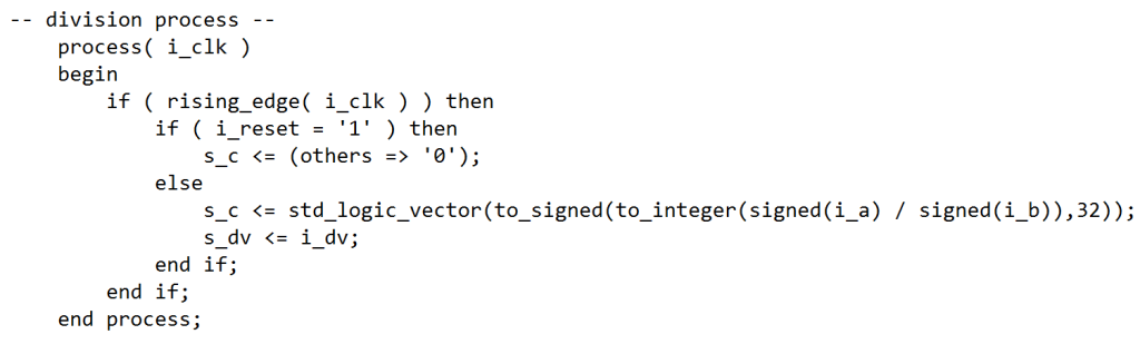
The above code, generates this schematic:
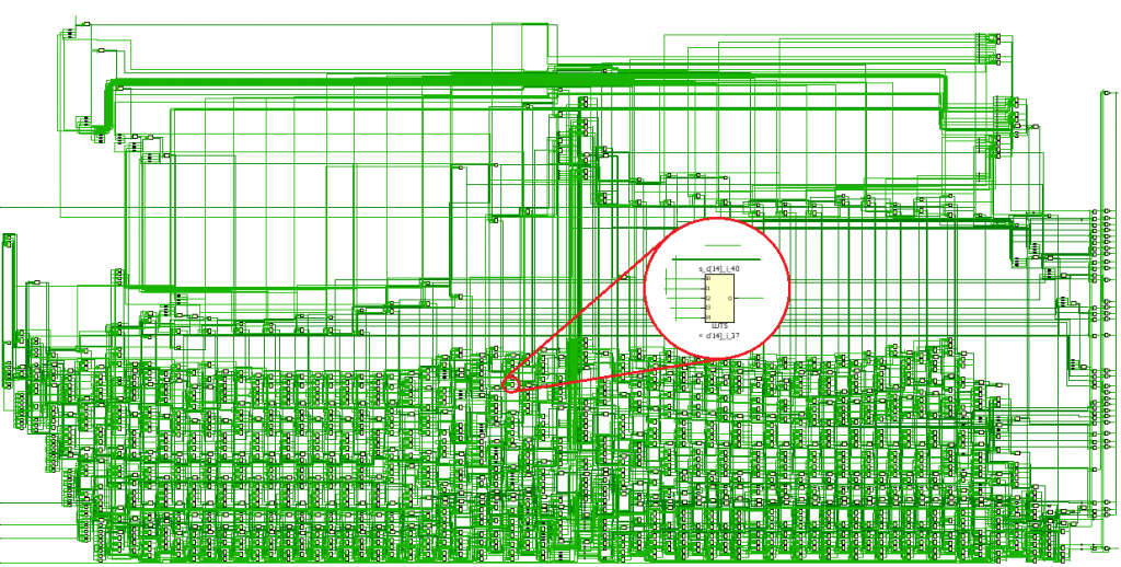
Vivado created a divider, as requested, but it took almost 1800 cells to do it. Meeting timing on this operation may prove to be very difficult, especially if it is a part of other logic operations that have to happen that clock cycle.
The Ugly
The Tools Aren’t Great
There is nothing quite like the frustration that comes from software tools that don’t do what you expect them to, or produce inconsistent results. Although commercial FPGAs have been around for quite some time, some aspects of the software ecosystems still are lacking. With the latest version of the Xilinx tools, Vivado, the industry has seen a large jump in functionality and features. However, since this tool is brand new and a near-complete rewrite of their legacy tools. It has its own set of challenges and bugs. Altera, the number two FPGA manufacturer, is still working with the same software package that they have been using for over a decade. To put that in perspective, that’s like running Windows ME today thinking that it was appropriate.
Debugging Timing Violations
Timing. Ugh. I’ve probably spent the most time being frustrated with FPGA design when it comes to some rough little bit of a netlist that just refuses to meet timing, no matter what I do to it. These little “show stoppers” come about all of the time. And the best way to squash them is simply with experience – there really isn’t much else that a designer can do. Xilinx has their UltraFast Design Methodology guide, and Altera copious amounts of documentation for “best practices,” but really when it comes down to it, it’s all about writing good, small, synthesizable HDL code. But no matter what, you’re going to find yourself in a situation where you need to instantiate 32 of something, and timing is going to be a nightmare. If you’d like to chat about your embedded needs, you can reach out to us here. Or, if you’d like more information on industrial embedded systems, check out our resources page.
Next Steps
If you’d like to chat about your industrial embedded needs, you can reach out to us here. Also, here’s some additional resources to help you on your journey:
- Custom Automated Test System Buyers Guide
- LabVIEW FPGA: The Good, the Bad, and the Ugly
- Outsourcing Industrial Embedded System Development Guide
- Need LabVIEW FPGA programming help? | LabVIEW FPGA Developers
- LabVIEW Industrial Automation Guide
- Industrial Embedded Design Resources – White Papers, Case Studies, Articles
- Automated Test System Resources – Webinars, White Papers, Case Studies, Articles